FIFO memory devices having write and read control circuits that support x4N, x2N and xN data widths during DDR and SDR modes of operation

Inactive Publication Date: 2005-02-24
INTEGRATED DEVICE TECH INC
View PDF54 Cites 36 Cited by
  • Summary
  • Abstract
  • Description
  • Claims
  • Application Information

AI Technical Summary

Benefits of technology

[0012] First-in first-out (FIFO) memory devices according to first embodiments of the present invention include a plurality of memory devices that are configured to support any combination of dual data rate (DDR) or single data rate (SDR) write modes that operate in-sync with a write clock signal (WCLK) and DDR or SDR read modes that operate in-sync with a read clock signal (RCLK). These FIFO memory devices also provide flexible x4N, x2N and xN bus matching on both read and write ports and enable data to be written an

Problems solved by technology

Because RWM devices use active circuitry to store data, they belong to a class of memory devices known as “volatile” memory devices because data stored therein will be lost upon termination of the power supply.
Because this latter type of data storage may be hardwired, the data cannot be modified, but can only be read.
However, the addition of ports to unit memory cells typically increases the complexity and layout area requirements for these higher bandwidth memory devices.
Unfortunately, a major disadvantage of typical dual-port SRAM-based FIFOs is the relatively large unit cell size for each dual-port SRAM cell therein.
Moreover, the relatively large unit cells of a dual-port SRAM FIF

Method used


Image

  • FIFO memory devices having write and read control circuits that support x4N, x2N and xN data widths during DDR and SDR modes of operation
  • FIFO memory devices having write and read control circuits that support x4N, x2N and xN data widths during DDR and SDR modes of operation
  • FIFO memory devices having write and read control circuits that support x4N, x2N and xN data widths during DDR and SDR modes of operation

Examples


Embodiment Construction

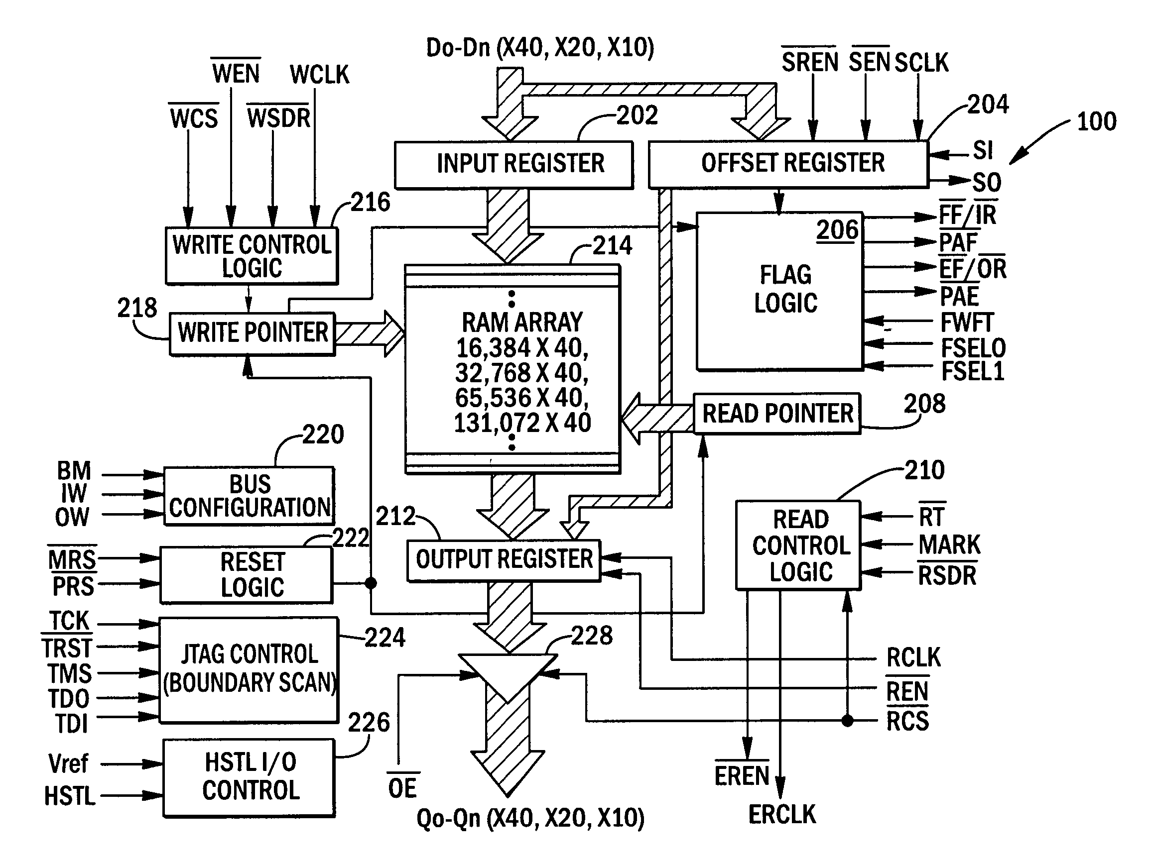
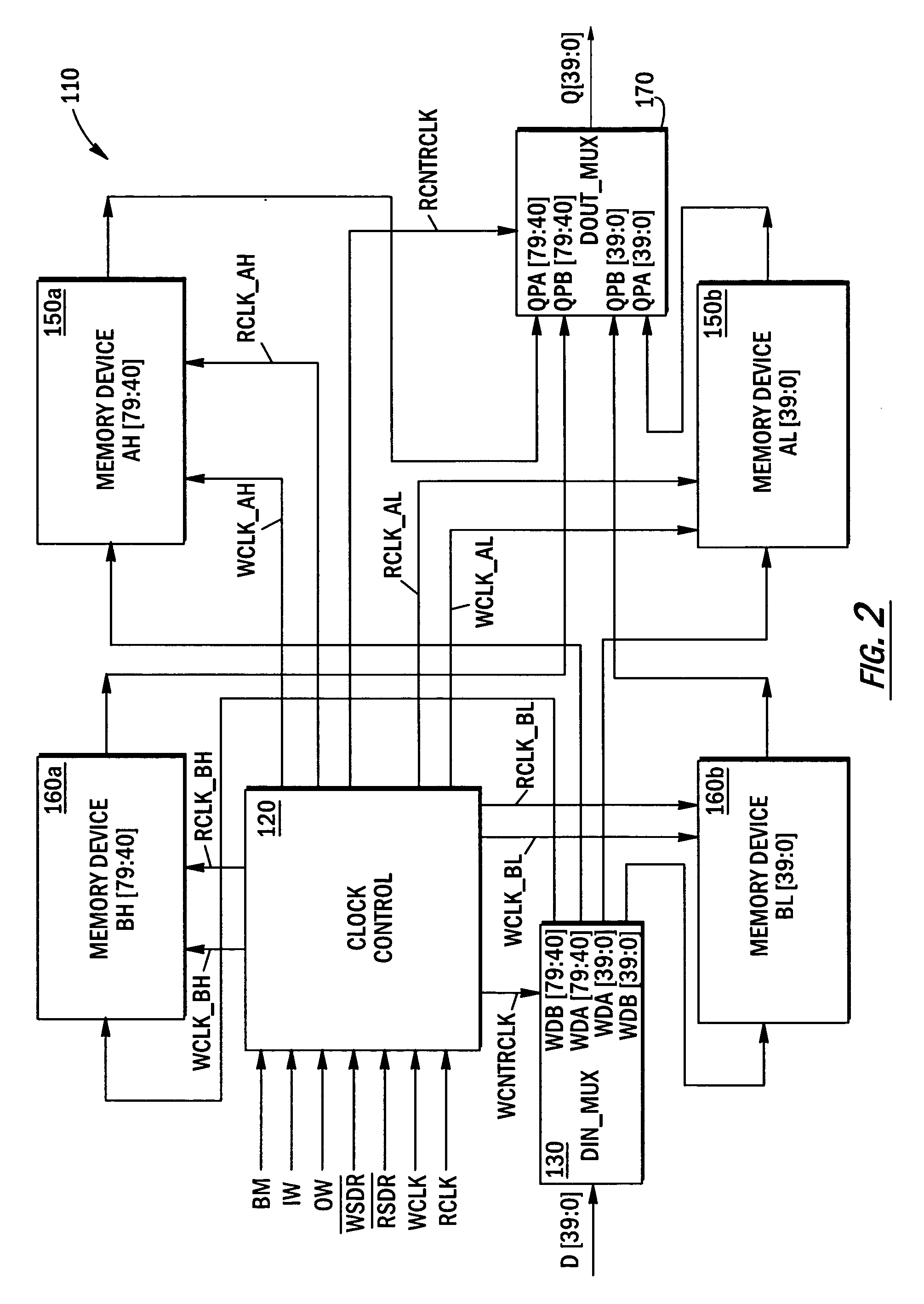
[0030] The present invention now will be described more fully with reference to the accompanying drawings, in which preferred embodiments of the invention are shown. This invention may, however, be embodied in many different forms and should not be construed as being limited to the embodiments set forth herein; rather, these embodiments are provided so that this disclosure will be through and complete, and will fully convey the scope of the invention to those skilled in the art. Like reference numerals refer to like elements throughout and signal lines and signals thereon may be referred to by the same reference characters. The prefix symbol “ / ” attached to a signal name indicates that the signal is an active low signal. Active low signals may be changed to active high signals and the description of such signals as active low signals should not be construed as limiting the embodiments described herein to the use of only such signals.

[0031] First-in first-out (FIFO) memory devices 1...


PUM


Abstract

First-in first-out (FIFO) memory devices are configured to support all four of the following FIFO memory modes: (1) DDR write with DDR read, (2) DDR write with SDR read, (3) SDR write with DDR read and (4) SDR write with SDR read. These FIFO memory devices provide flexible x4N, x2N and xN bus matching on both read and write ports and enable data to be written and read on both rising and falling edges of the write and read clock signals. Custom flag generation and retransmit circuitry is also provided that can efficiently handle any width DDR write mode with any width SDR read mode or any width SDR write mode with any width DDR read mode.

Description

REFERENCE TO PRIORITY APPLICATION [0001] This application is a continuation of U.S. application Ser. No. 10 / 459,224, filed Jun. 11, 2003, which is a continuation of U.S. application Ser. No. 09 / 972,265, filed Oct. 5, 2001, which claims priority to U.S. Provisional Application Ser. No. 60 / 314,393, filed Aug. 23, 2001, the disclosures of which are hereby incorporated herein by reference.FIELD OF THE INVENTION [0002] The present invention relates to integrated circuit memory devices and, more particularly, to integrated circuit first-in first-out (FIFO) memory devices. BACKGROUND OF THE INVENTION [0003] Semiconductor memory devices can typically be classified on the basis of memory functionality, data access patterns and the nature of the data storage mechanism. For example, distinctions are typically made between read-only memory (ROM) devices and read-write memory (RWM) devices. The RWM devices typically have the advantage of offering both read and write functionality with comparable...

Claims


Application Information

Patent Timeline
IPC IPC(8): G06F5/06
CPCG06F2205/062G06F5/06
Inventor DUH, JIANN-JENGAU, MARIO FULAM
Owner INTEGRATED DEVICE TECH INC
Why Eureka
Try Eureka