Non-volatile RAM cell and array using nanotube switch position for information state

a technology of information state and nanotubes, applied in static storage, digital storage, instruments, etc., can solve the problems of long write cycles (ms), low relative speed of dram or sram, and relatively low cost of rom,

Active Publication Date: 2005-02-24
NANTERO
View PDF47 Cites 100 Cited by
  • Summary
  • Abstract
  • Description
  • Claims
  • Application Information

AI Technical Summary

Problems solved by technology

ROM is relatively low cost but cannot be rewritten.
EEPROM (or “Flash”) is inexpensive, and has low power consumption but has long write cycles (ms) and low relative speed in comparison to DRAM or SRAM.
Flash also has a finite number of read/write cycles leading to low long-term reliability.
SRAM does not need to be refreshed and is fast relative to DRAM, but has lower density and is more expensive relative to DRAM.
Both SRAM and DRAM are volatile, meaning that if power to the memory is interrupted the memory will lose the information stored in the memory cells.
Consequently, existing technologies are either non-volatile but are not randomly accessible and have low density, high cost, and limited ability to allow multiples writes with high reliability of the circuit's function, or they are volatile and complicate system design or have low density.
A different memory cell based upon magnet...

Method used


Image

  • Non-volatile RAM cell and array using nanotube switch position for information state
  • Non-volatile RAM cell and array using nanotube switch position for information state
  • Non-volatile RAM cell and array using nanotube switch position for information state

Examples


Embodiment Construction

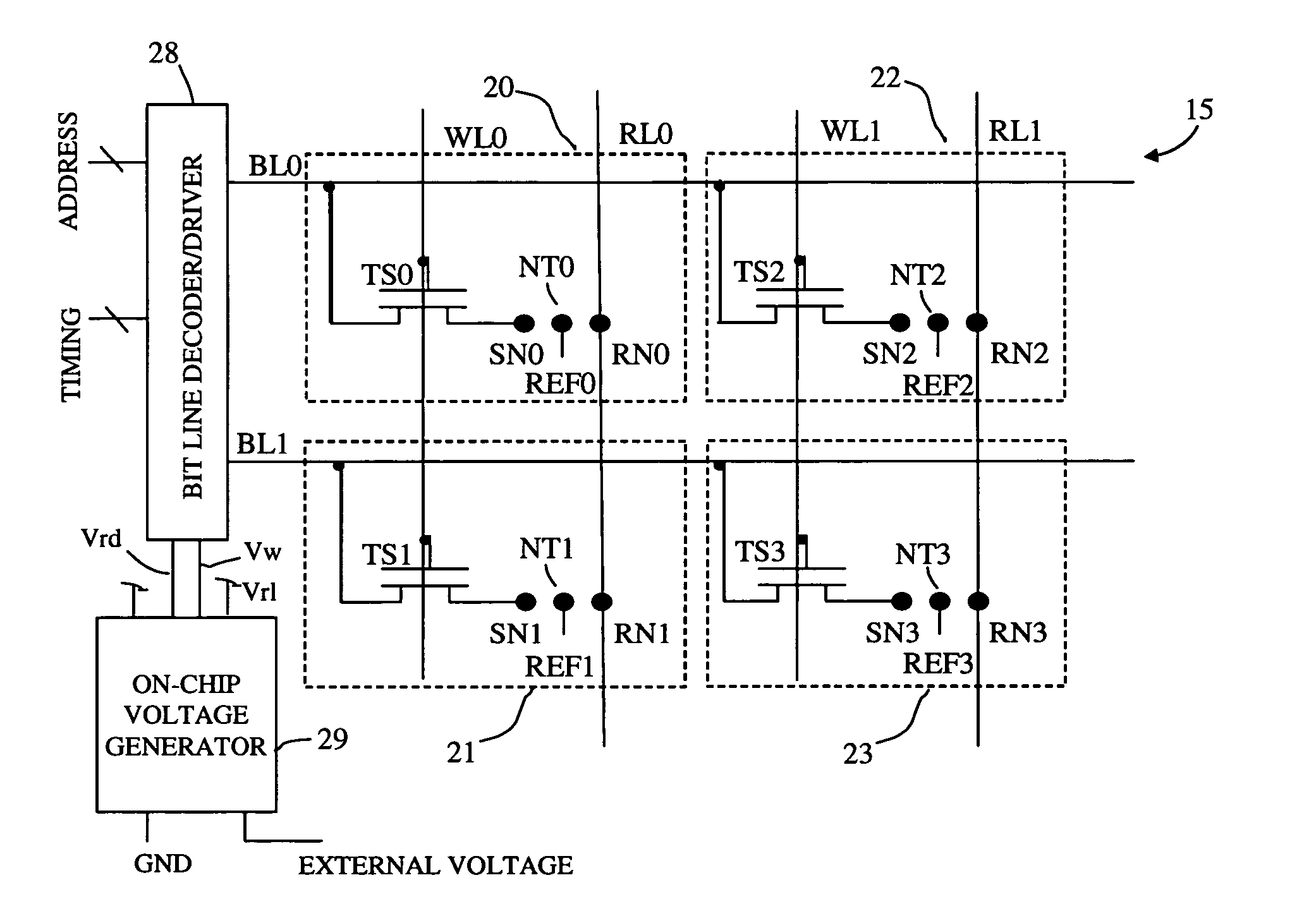
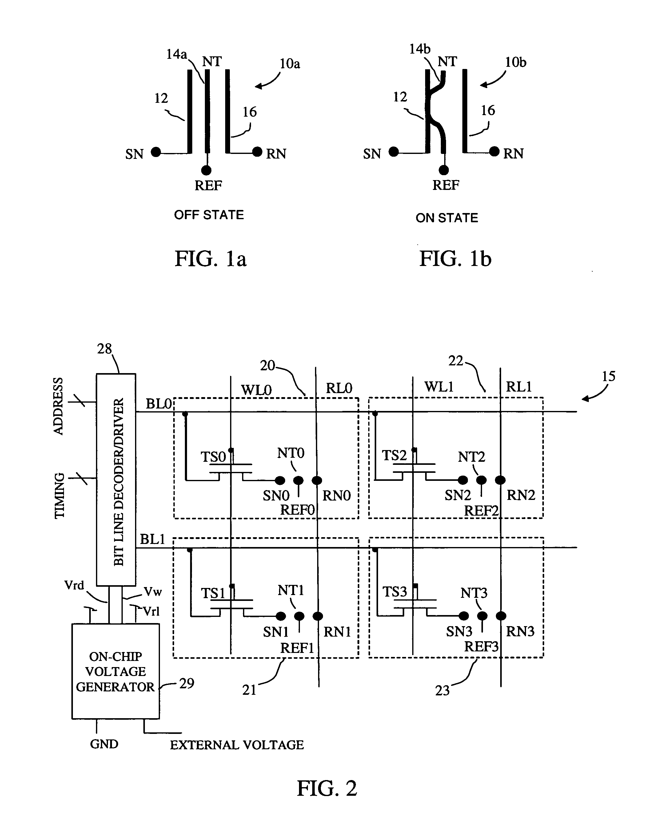
[0036] One embodiment of an NT switching component includes NFET or PFET devices, particularly NFET array devices in combination with nanotube (NT) electromechanical switching components to provide unit cells that may be employed in integrated circuits. The NT switching component has two states: an “ON” state and an “OFF” state. As shown in FIG. 1a, the OFF state 10a has an un-deflected NT 14a, resulting in an open circuit (i.e., high impedance in the range of one or more mega-ohms) between NT 14a and select electrode 12 connected to terminal SN, and release electrode 16 connected to node RN. Alternatively, the “OFF” state may have a deflected NT in contact with an insulating layer on node RN (not shown). In this OFF state, a small parasitic capacitance exists between NT 14a and select electrode 12 and release electrode 16. In the ON state 10b as shown in FIG. 1b, NT 14b is flexed and held in close proximity to a select node (electrode) by van der Waal forces, resulting in an ohmic ...


PUM


Abstract

Non-Volatile RAM Cell and Array using Nanotube Switch Position for Information State. A non-volatile memory array includes a plurality of memory cells, each cell receiving a bit line, word line, and release line. Each memory cell includes a cell selection transistor with first, second and third nodes. The first and second nodes are in respective electrical communication with the bit line and the word line. Each cell further includes an electromechanically deflectable switch, having a first, second and third node. The first node is in electrical communication with the release line, and a third node is in electrical communication with the third node of the cell selection transistor. The electromechanically deflectable switch includes a nanotube switching element physically positioned between the first and third nodes of the switch and in electrical communication with the second node of the switch. The second node of the switch is in communication with a reference signal. Each nanotube switching element is deflectable into contact with the third node of the switch in response to signals at the first and second node of the cell selection transistor and is releasable from such contact in response to a signal at the release line. In preferred embodiments, the cell selection transistor is a FET and the second node of the transistor is a gate of the FET.

Description

CROSS-REFERENCE TO RELATED APPLICATIONS [0001] This application claims priority under 35 U.S.C. §119(e) to U.S. Provisional Pat. Apl., Ser. No. 60 / 459,222, filed on Mar. 28, 2003, entitled NRAM Byte / Block Released Bit Selectable One-Device Nanotube Array, which is incorporated herein by reference in its entirety. [0002] This application is related to the following U.S. applications, the contents of which are incorporated herein in their entirety by reference: [0003] U.S. Provisional Apl. Ser. No. 60 / 459,223 filed on Mar. 28, 2003, entitled NRAM Bit Selectable Two-Device Nanotube Array; and U.S. Pat. Apl., Ser. No. (inserted upon USPTO designation), filed on the same day as the present application, entitled NRAM Bit Selectable Two-Device Nanotube Array. [0004] U.S. Provisional Patent Application No. 60 / 459,253, filed on Mar. 28, 2003, entitled Single Transistor with Integrated Nanotube (NT-FET); and U.S. Pat. Apl, Ser. No. (inserted upon USPTO designation), filed on the same day as t...

Claims


Application Information

Patent Timeline
IPC IPC(8): G11C13/02G11C23/00
CPCB82Y10/00G11C23/00G11C13/025
Inventor RUECKES, THOMASSEGAL, BRENT M.VOGELI, BERNHARDBROCK, DARRENJAIPRAKASH, VENKATACHALAM C.BERTIN, CLAUDE L.
Owner NANTERO
Why Eureka
Try Eureka