Reservation of design elements in a parallel printed circuit board design environment

a design environment and parallel printed circuit board technology, applied in the field of electronic design automation tools, can solve the problems of user limited viewing only areas, user cannot see edits made to the rest of the board while user is on the board, etc., and achieve the effect of increasing the size of the boundary

Active Publication Date: 2005-02-24
SIEMENS PROD LIFECYCLE MANAGEMENT SOFTWARE INC
View PDF94 Cites 34 Cited by
  • Summary
  • Abstract
  • Description
  • Claims
  • Application Information

AI Technical Summary

Benefits of technology

Embodiments of the invention include methods for simultaneous editing of at least a portion of a printed circuit board (PCB) design by multiple users. Such methods include receiving design data at each of first and second clients. The design data includes graphically displayable information regarding a pattern of electronic components and connections between those components for at least a portion of the design. The design data also includes data corresponding to at least a portion of a shared area of the design, and the shared area is simultaneously editable by both of the clients. The method fur

Problems solved by technology

Using the above-described approach, a user is limited to viewing only areas of the design that are opened by that user

Method used


Image

  • Reservation of design elements in a parallel printed circuit board design environment
  • Reservation of design elements in a parallel printed circuit board design environment
  • Reservation of design elements in a parallel printed circuit board design environment

Examples


example shared pcb

Editing Environment

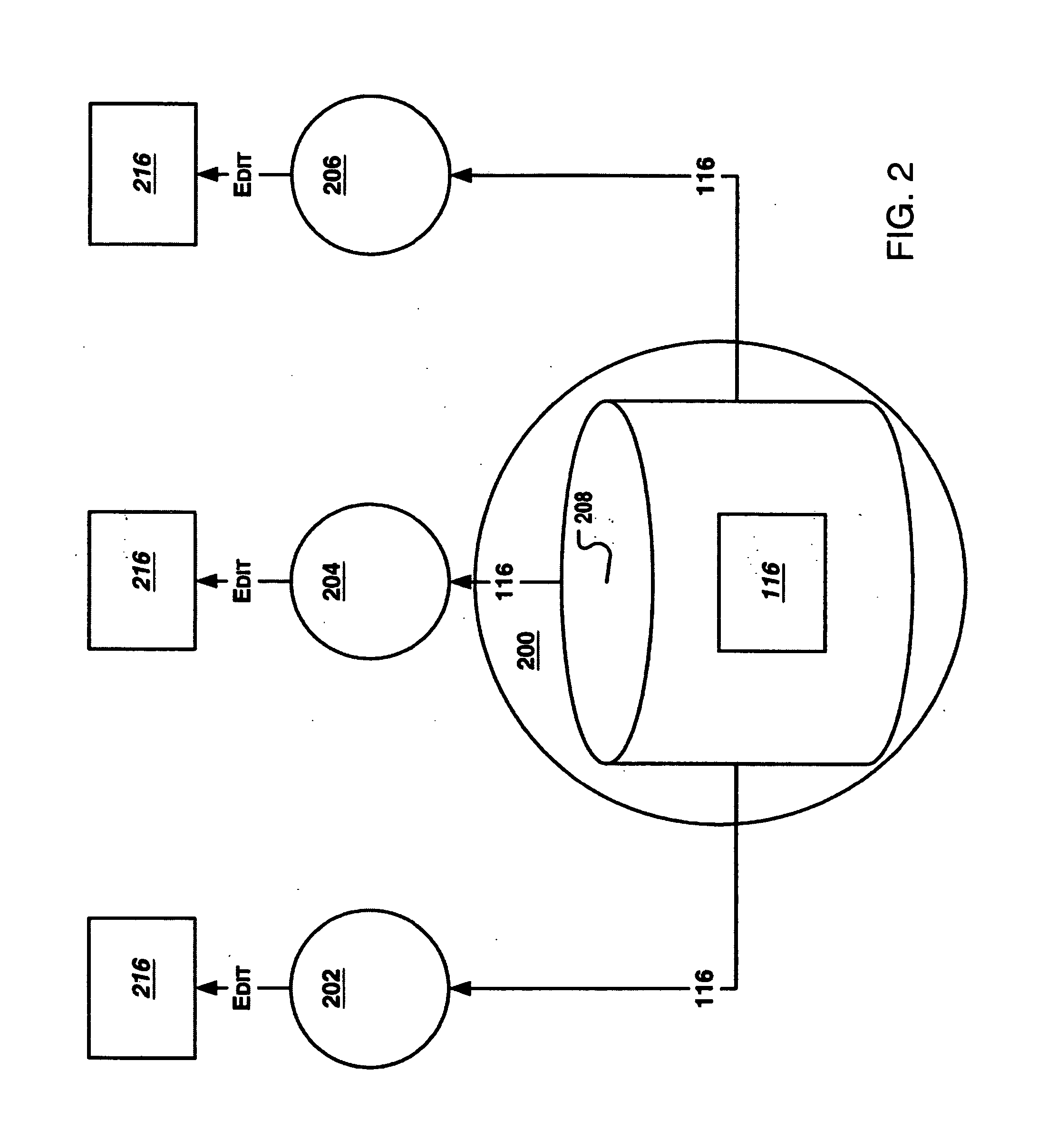
FIG. 15 is a conceptual diagram illustrating a shared simultaneous editing environment according to at least one embodiment of the invention. A design session manager (or server) communicates in a networked environment with multiple design clients (clients A, B and C) operated by multiple users (users A, B and C). The server maintains a database containing the master PCB design. The database may be located at the server or elsewhere in the network (e.g., “data” in FIG. 15). Software executed by the server receives edit requests from each client, and checks each request to ensure it will not conflict with another edit or otherwise cause a design rule violation. If an edit request does not conflict or otherwise violate a design rule, the server accepts the edit and synchronizes each client to include that edit. Each client has a processor and memory. Each client is able to view the entire design, as well as edits corresponding to server-accepted edit requests from o...


PUM


Abstract

Multiple users simultaneously edit at least a portion of a printed circuit board (PCB) design. The PCB design portion is transmitted to first and second clients for graphical display at each of the clients. A first protection boundary is associated with an area of the PCB design being edited at the first client. A second protection boundary is associated with an area of the PCB design being edited at the second client. The first and second protection boundaries are displayed at each of the first and second clients. A request from one of the clients to edit an object within a region bounded by a protection boundary associated with the other client is rejected. The protection boundary may surround a user's cursor. The size of the boundary may increase based on editing activity by a user in an area of a PCB design.

Description

COPYRIGHT NOTICE A portion of the disclosure of this patent document may contain material which is subject to copyright protection. To the extent that it does, the copyright owner has no objection to the facsimile reproduction by anyone of the patent document or the patent disclosure as it appears in the Patent and Trademark Office patent file or records, but otherwise reserves all copyright rights whatsoever. The following notice applies to the software and data as described below and in the drawings hereto: Copyright © 2003-2004, Mentor Graphics Corp., All Rights Reserved. FIELD OF THE INVENTION This invention relates to the field of electronic design automation tools, and more specifically, to a mechanism for facilitating ease of use and conflict avoidance in a shared environment for parallel printed circuit board (PCB) design. BACKGROUND OF THE INVENTION A printed circuit board (“PCB”) often begins as a schematic diagram by which an electrical engineer describes an electronic...

Claims


Application Information

Patent Timeline
IPC IPC(8): G06F17/30G06F17/50
CPCG06F2217/04G06F17/5068G06F2111/02G06F30/39
Inventor PETUNIN, VLADIMIR V.PFEIL, CHARLES L.POTTS, HENRYSHIKALOV, VLADIMIR B.
Owner SIEMENS PROD LIFECYCLE MANAGEMENT SOFTWARE INC
Why Eureka
Try Eureka