Protected organic electronic device structures incorporating pressure sensitive adhesive and desiccant

a technology of organic electronic devices and desiccant, applied in the direction of thermoelectric devices, organic semiconductor devices, semiconductor/solid-state device details, etc., can solve the problems of limiting the lifetime of the device, reducing the service life of the device, so as to minimize the undesirable contact between the getter and the effect of damage to the organic electronic device region

Inactive Publication Date: 2005-03-03
UNIVERSAL DISPLAY
View PDF11 Cites 87 Cited by
  • Summary
  • Abstract
  • Description
  • Claims
  • Application Information

AI Technical Summary

Benefits of technology

[0019] An advantage of the present invention is that organic electronic structures are provided, which are effective in protecting sensitive device components from oxygen, moisture and other harmful species in the surrounding atmosphere.
[0020] Another advantage of the present invention is that organic electronic structures are provided, which afford protection from these harmful species, while at the same time being flexible and conformable to other surfaces, if desired.
[0021] Another advantage of the present invention is that organic electronic structures are provided, which are amenable to continuous processing techniques, such as web-based (e.g., roll-to-roll) manufacturing methods.
[0022] Still other advantages accrue from the fact that the adhesive layer is disposed over the entire organic electronic device region.
[0023] For example, it is known in the organic electronic device art to provide a getter material within a rigid cover, with the getter material being separated from the organic electronic device region by an air gap. In general, the present inventors have found that it is desirable to position the getter as close as is possible to the organic electronic device region. However, certain getter materials produce potentially harmful byproducts (e.g., acids) upon reacting with gaseous species from the outside environment (e.g., water). By covering the entire organic electronic device region with adhesive, however, the organic electronic device region is isolated from such harmful species, allowing the getter region to be positioned in close proximity to the organic electronic device region. At the same time, all adhesives, including the pressure-sensitive adhesive layers used herein, have an associated non-zero permeation rate. Accordingly the presence of the getter material is beneficial in that it absorbs harmful species as they permeate through the adhesive layer.
[0024] As another example, even if the getter material utilized does not produce potentially harmful byproducts, when dealing with a flexible device, the presence of a narrow air gap between the getter and the organic electronic device region affords little to no protection of the organic electronic device region during flexing, and damage to the organic electronic device region can occur due to contact between the organic electronic device region and the getter. By covering the entire organic electronic device region with adhesive, however, undesirable contact between the getter and the organic electronic device region is minimized, thereby protecting the organic electronic device region from such damage.

Problems solved by technology

Low work function metals, however, are chemically reactive; exposure to and subsequent reaction with oxygen and moisture can severely limit the lifetime of the devices.
Moisture and oxygen are also known to produce other deleterious effects, for instance, reactions with the organic materials themselves.
Epoxy resins, however, are typically not flexible, rendering these materials undesirable for use in connection with flexible OLEDs.
In addition, because they are typically inflexible, because they are not pressure sensitive, and because they are typically applied in liquid form, epoxy resins are not readily adaptable for use in web-based manufacturing techniques.
Moreover, epoxy resins frequently contain ingredients that are deleterious to OLEDs.
Analogous difficulties are encountered in organic electronic devices other than OLEDs.
Although such adhesive layers do provide a degree of protection from the outside environment, the barrier properties of these adhesive layers are often insufficient to protect the OLED device from premature degradation in commercial applications.

Method used


Image

  • Protected organic electronic device structures incorporating pressure sensitive adhesive and desiccant
  • Protected organic electronic device structures incorporating pressure sensitive adhesive and desiccant
  • Protected organic electronic device structures incorporating pressure sensitive adhesive and desiccant

Examples


Embodiment Construction

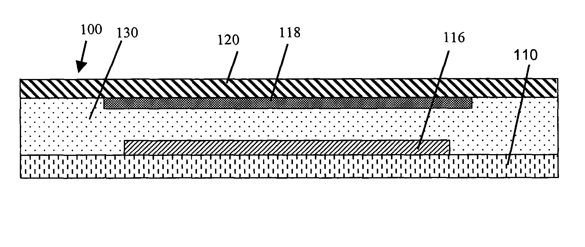
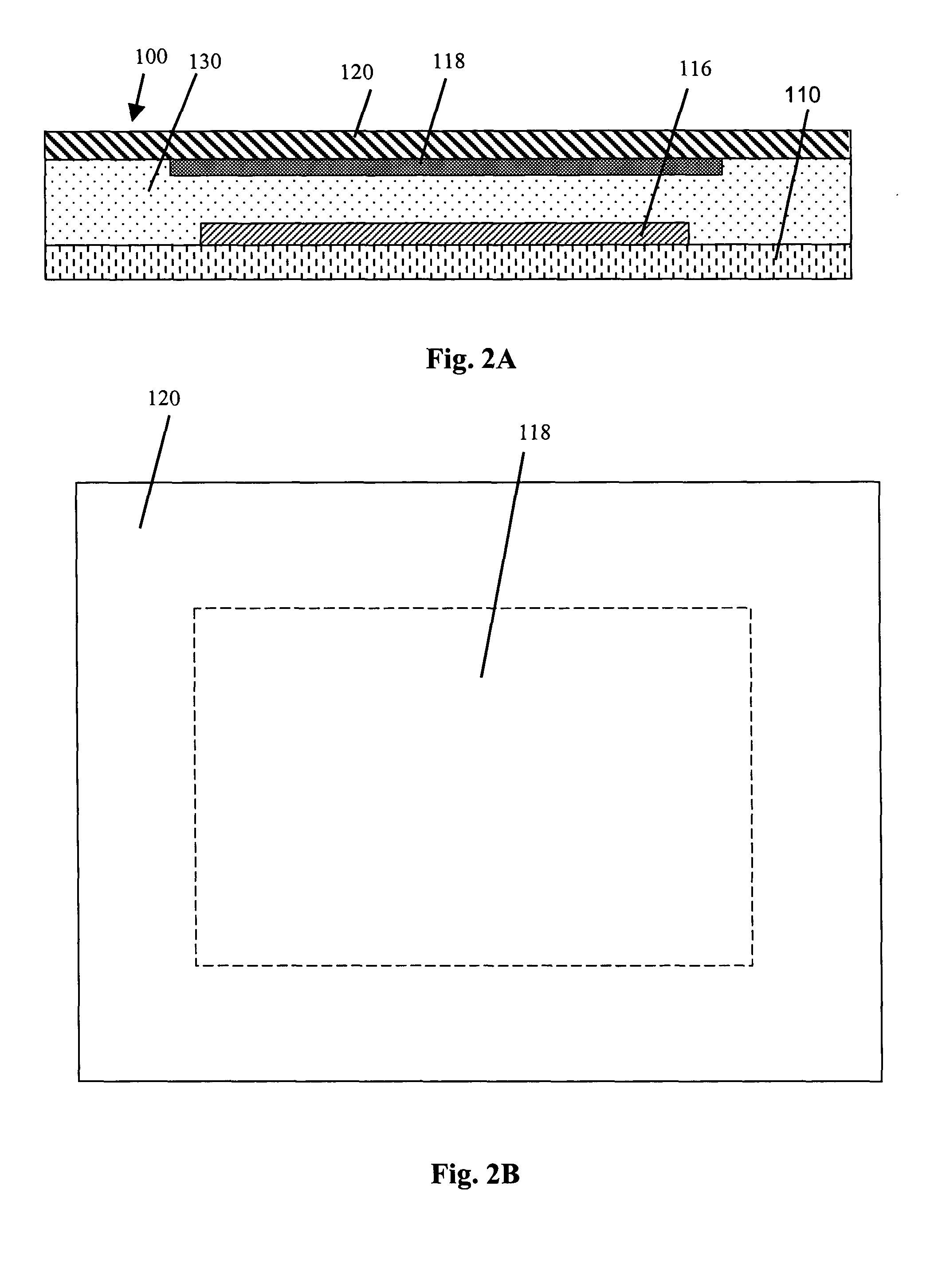
[0033] The present invention now will be described more fully hereinafter with reference to the accompanying drawings in which preferred embodiments of the invention are shown. This invention may, however, be embodied in different forms and should not be construed as limited to the embodiments set forth herein. For example, although the embodiments below are directed to OLED structures, the techniques and structures of the present invention are applicable to other organic electronic device structures as well.

[0034] As used herein, a “layer” of a given material includes a region of that material where the thickness is small compared to both its length and width. Examples of layers include sheets, foils, films, laminations, coatings, and so forth. As used herein, a layer need not be planar, but can be bent, folded or otherwise contoured, for example, to at least partially, or even completely, envelop another component. As used herein, a layer can also include multiple sub-layers. As ...


PUM


Abstract

Organic electronic device structures are provided, which comprise: (a) a first portion comprising a substrate and an organic electronic device region (e.g., an OLED region) disposed over the substrate; (b) a second portion comprising a cover and a getter region; and (c) a radiation-curable, pressure-sensitive adhesive layer disposed between the first and second portions and adhering the first and second portions to one another. The adhesive layer is disposed over the entire organic electronic device region and over at least a portion of the substrate. Other aspects of the present invention are directed to methods of making the above structures.

Description

STATEMENT OF RELATED APPLICATION [0001] This application is related to U.S. application Ser. No. 10 / 407,820 filed Apr. 4, 2003 and to U.S. application Ser. No. 10 / 122,969 filed Apr. 12, 2002, both entitled “Protected Organic Electronic Devices and Methods for making the same.”FIELD OF THE INVENTION [0002] The present invention relates to organic electronic devices that are protected from environmental elements such as moisture and oxygen. BACKGROUND OF THE INVENTION [0003] Organic electronic devices including circuits, for example, organic light emitting diodes, organic electrochromic displays, organic photovoltaic devices and organic thin film transistors, are known and are becoming increasingly important from an economic standpoint. [0004] As a specific example, organic light emitting devices (“OLEDs”), including both polymer and small-molecule OLEDs, are potential candidates for a great variety of virtual- and direct-view type displays, such as lap-top computers, televisions, dig...

Claims


Application Information

Patent Timeline
Patent Type & Authority Applications(United States)
IPC IPC(8): H01L21/00H01L33/00H01L51/52
CPCH01L51/5237Y10S257/913H01L2251/5338H10K50/846H10K50/8426H10K50/8445H10K2102/311
Inventor SILVERNAIL, JEFFREY ALAN
Owner UNIVERSAL DISPLAY
Why Eureka
Try Eureka