Integrated circuit device having input/output electrostatic discharge protection cell equipment with electrostatic discharge protection element and power clamp

a protection element and integrated circuit technology, which is applied in the direction of circuit arrangement, emergency protection circuit arrangement, emergency protection circuit arrangement for limiting excess voltage/current, etc., can solve the problems of increasing complexity of the fabricating process, increasing the size of the integrated circuit device, and difficulty in meeting esd protection characteristics in a given area

Inactive Publication Date: 2005-03-03
SAMSUNG ELECTRONICS CO LTD
View PDF14 Cites 85 Cited by
  • Summary
  • Abstract
  • Description
  • Claims
  • Application Information

AI Technical Summary

Benefits of technology

[0009] The present invention provides an integrated circuit device having an I / O ESD protection cell that occupies a small area and performs an ESD protection function.

Problems solved by technology

While ESD evaluation standards are the same irrespective of the type of integrated circuit device, the size of the integrated circuit device becomes increasingly small and the fabricating process becomes increasingly complicated as the degree of integration of the integrated circuit device becomes higher.
Accordingly, it becomes difficult to satisfy ESD protection characteristics in a given area.

Method used


Image

  • Integrated circuit device having input/output electrostatic discharge protection cell equipment with electrostatic discharge protection element and power clamp
  • Integrated circuit device having input/output electrostatic discharge protection cell equipment with electrostatic discharge protection element and power clamp
  • Integrated circuit device having input/output electrostatic discharge protection cell equipment with electrostatic discharge protection element and power clamp

Examples


first embodiment

[0070]FIG. 4A is a schematic diagram showing an integrated circuit device 100 according to the present invention. FIGS. 4B and 4C show layouts of an I / O ESD protection cell 130. FIG. 4D is a sectional view taken along the D-D′ line of FIG. 4C.

[0071] The integrated circuit device 100 comprises the I / O ESD protection cell 130 for each I / O pad 90. The ESD protection cell 130 may be located beside the I / O pad 90, or at least a portion or all of the ESD protection cell 130 may be located below the I / O pad 90, which will be described later. The pitch P and height H of the I / O ESD protection cell 130 are determined depending on the pitch P and height H of the I / O pad 90.

[0072] In FIGS. 4B and 4C, the pitches of the I / O ESD protection cells 130 are the same, but the heights are different from each other. When the height H1 is small, as shown in FIG. 4B, the area of the I / O ESD protection cell 130 should be made smaller. However, when the height H2 is large, as shown in FIG. 4C, the area of...

second embodiment

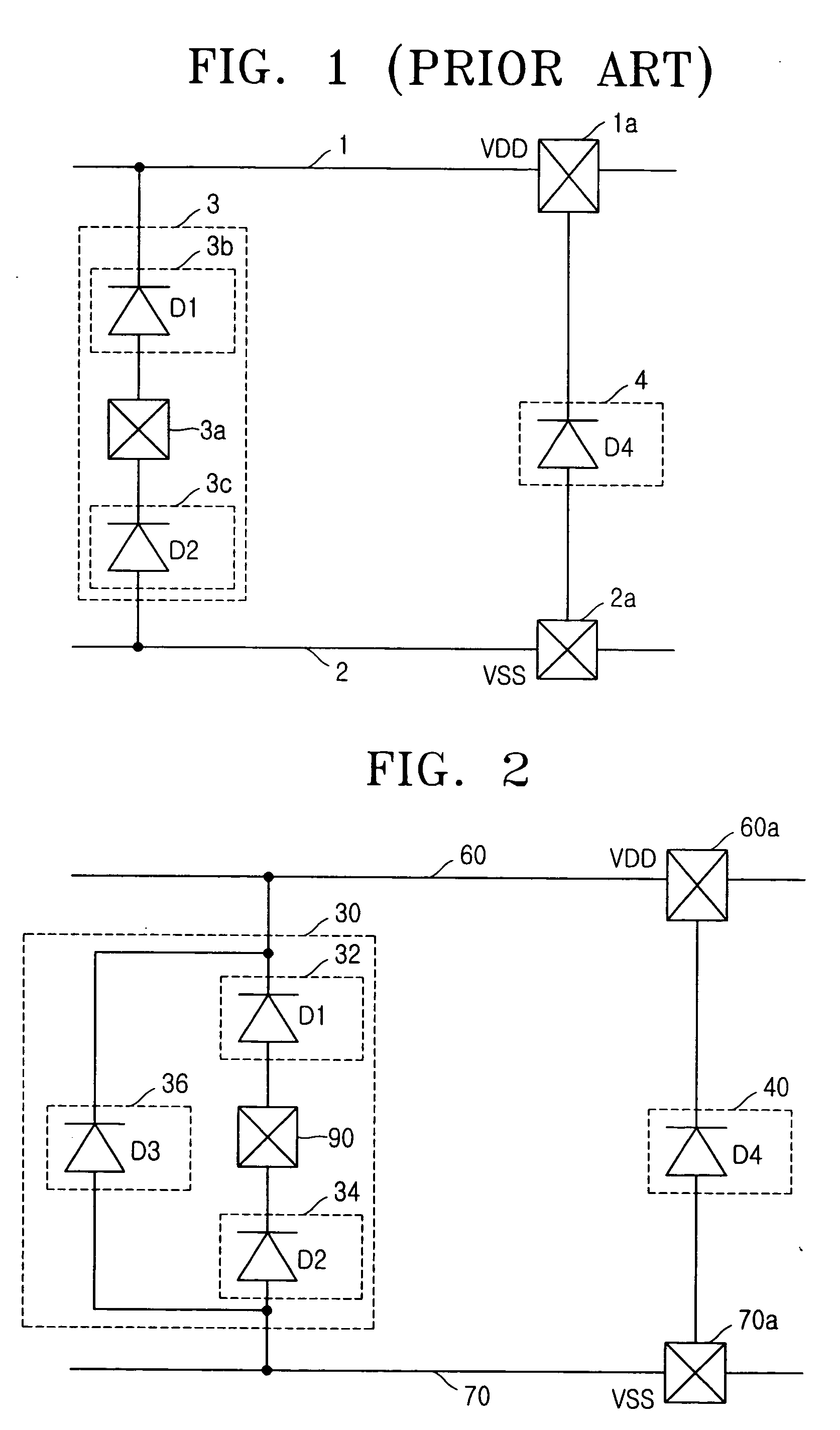
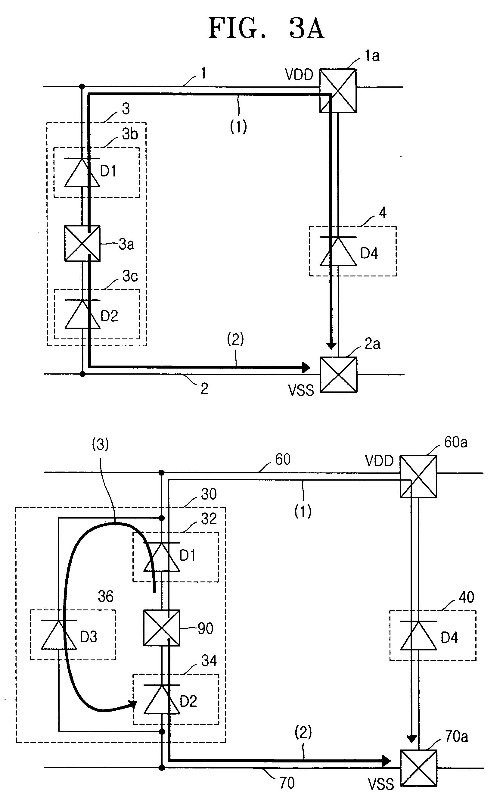
[0089] In the second embodiment, the power clamp element 236 is separated from the protection elements 232 and 234, whereby an effect of a parasitic ESD current path can be prevented. In addition, the N-well 110 surrounds the N+ active region 115, whereby the efficiency of the power clamp element 236 increases.

[0090]FIG. 10 is a sectional view showing a modified example 200′ of the second embodiment where a VSS ESD protection element 234 is formed in a P-well 120 without an N-well. If a desired ESD protection function is achieved only by regulating process conditions for forming the VSS ESD protection element 234, as shown in FIG. 10, the N-well does not need to be formed.

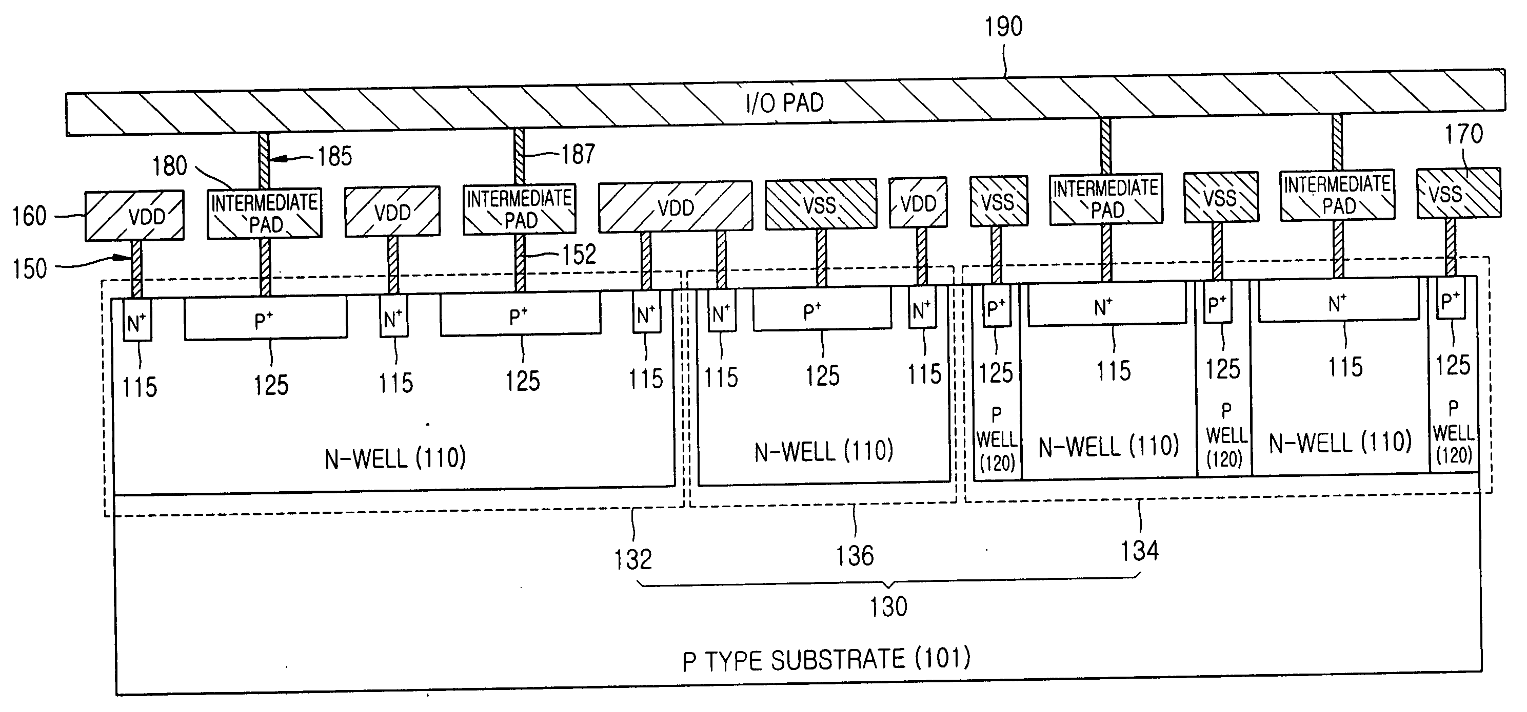
[0091]FIG. 11A shows a layout of an I / O ESD protection cell 330 constituting an integrated circuit device 300 according to a third embodiment of the present invention, and FIG. 11B is a sectional view taken along the B-B′ line of FIG. 11A. The I / O ESD protection cell 330 of the third embodiment is different from t...

fourth embodiment

[0094]FIG. 13A shows a layout of an I / O ESD protection cell 430 constituting an integrated circuit device 400 according to the present invention, and FIG. 13B is a sectional view taken along the B-B′ line of FIG. 13A.

[0095] The I / O ESD protection cell 430 of the fourth embodiment is different from that of each of the first through third embodiments in that a power clamp element 436, a VDD ESD protection element 432, and a VSS ESD protection element 434 comprise MOS transistors.

[0096] As shown in circuit diagrams of FIG. 13B, when each of the VDD ESD protection element 432 and the VSS ESD protection element 434 comprises two MOS transistors connected to each other in parallel, the ESD current path is divided and the ESD protection function is thus improved. While the drawings have illustrated a case where two MOS transistors are connected to each other in parallel, if possible, more than two MOS transistors are preferably connected to one another in parallel.

[0097] In the I / O ESD c...


PUM


Abstract

There is provided an integrated circuit device having an input/output electrostatic discharge (I/O ESD) protection cell. The integrated circuit device includes an I/O ESD protection cell comprising a VDD ESD protection element connected between an I/O pad and a VDD line, a ground voltage (VSS) ESD protection element connected between the I/O pad and a VSS line, and a power clamp element connected between the VDD line and the VSS line, and wherein the VDD ESD protection element, the power clamp element, and the VSS ESD protection element in the I/O ESD protection cell are adjacent to each other so they can be connected in a straight line or are arranged to partially overlap.

Description

BACKGROUND OF THE INVENTION [0001] This application claims the priority of Korean Patent Application No. 2003-59483, filed on Aug. 27, 2003, in the Korean Intellectual Property Office, the disclosure of which is incorporated herein in its entirety by reference. [0002] 1. Field of the Invention [0003] The present invention relates to an integrated circuit device having an electrostatic discharge (ESD) protection circuit, and more particularly, to an integrated circuit device having an input / output (I / O) ESD protection cell that occupies a small area and performs an ESD protection function. [0004] 2. Description of Related Art [0005] In general, ESD protection levels are determined by the composition of an ESD protection circuit, a layout for realizing the ESD protection circuit in an actual integrated circuit device, and a fabricating process used to fabricate the integrated circuit device. While ESD evaluation standards are the same irrespective of the type of integrated circuit dev...

Claims


Application Information

Patent Timeline
Patent Type & Authority Applications(United States)
IPC IPC(8): H01L27/04H01L21/82H01L21/822H01L23/60H01L23/62H01L27/02H01L29/72H01L29/74H01L31/062H01L31/111
CPCH01L27/0251H01L27/04
Inventor KIM, HAN-GULEE, KI-TAEKO, JAE-HYOKKIM, WOO-SUBJANG, SUNG-PIL
Owner SAMSUNG ELECTRONICS CO LTD
Why Eureka
Try Eureka