Reference voltage detector for power-on sequence in a memory

Inactive Publication Date: 2005-03-03
POLARIS INNOVATIONS
View PDF11 Cites 4 Cited by
  • Summary
  • Abstract
  • Description
  • Claims
  • Application Information

AI Technical Summary

Benefits of technology

[0010] In accordance with a preferred embodiment of the present invention, a circuit comprising a latch having an input coupled to a reference voltage signal input, the latch containing circuitry to detect when the input rises to a specified level and asserting a clock enable signal when the input rises to the specified level, and a filter having an input coupled to an output of the latch and an output coupled to the latch, the filter containing circuitry to eliminate transients from a signal at its input.
[0011] In accordance with another preferred embodiment of the present invention, a circuit comprising a latch having an input coupled to a reference voltage signal input, the latch for use in tracking the reference voltage signal input, and a filter having an input coupled to the output of the latch, the filter for use in eliminating transients from a signal at its input.
[0012] An advantage of a preferred embodiment of the present invention is that the reference voltage signal is ensured of being at the desired level prior to the memory beginning operation. This can prevent the misdetection of data stored in memory elements.
[0013] A further advantage of a preferred embodiment of the present invention is that glitches and noise can be filtered while adherence to strict performance requirements is still met. This ensures interoperability with electronic equipment expecting a certain level of performance.

Problems solved by technology

If the reference voltage signal is not at the proper value, then the comparisons made with the differential inputs can result in erroneous assignment of data stored in memory elements.
However, by the time the memory begins operations, the glitch has disappeared and VREF is no longer at the proper value.
One disadvantage of the first prior art method is that the “CHIP ready” signal may be generated accidentally after receiving a random command sequence which may happen to fit the power-up sequence.
A second disadvantage of the first prior art method is that the “CHIP ready” signal can interfere with circuitry in the memory and may result in unwanted and unexpected states.
A disadvantage of the second prior art method is that the DDR SDRAM specifications require a fast detection and does not allow for most kinds of filtering operations that would prevent glitches and / or noise on CKE.

Method used


Image

  • Reference voltage detector for power-on sequence in a memory
  • Reference voltage detector for power-on sequence in a memory
  • Reference voltage detector for power-on sequence in a memory

Examples


Embodiment Construction

[0021] The making and using of the presently preferred embodiments are discussed in detail below. It should be appreciated, however, that the present invention provides many applicable inventive concepts that can be embodied in a wide variety of specific contexts. The specific embodiments discussed are merely illustrative of specific ways to make and use the invention, and do not limit the scope of the invention.

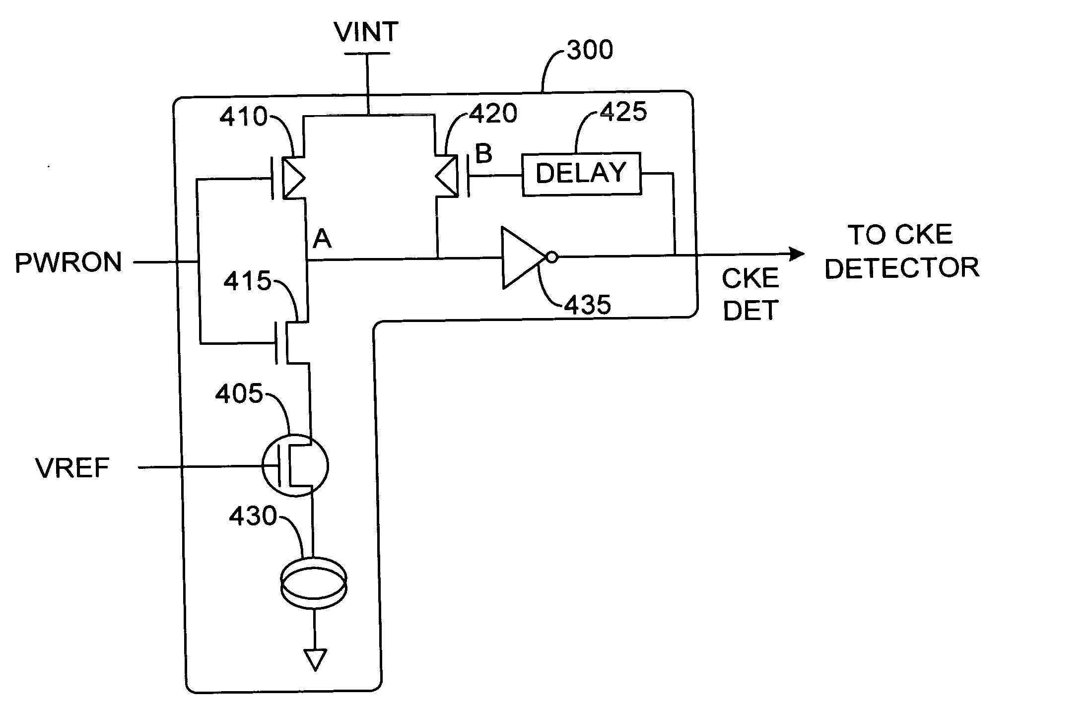
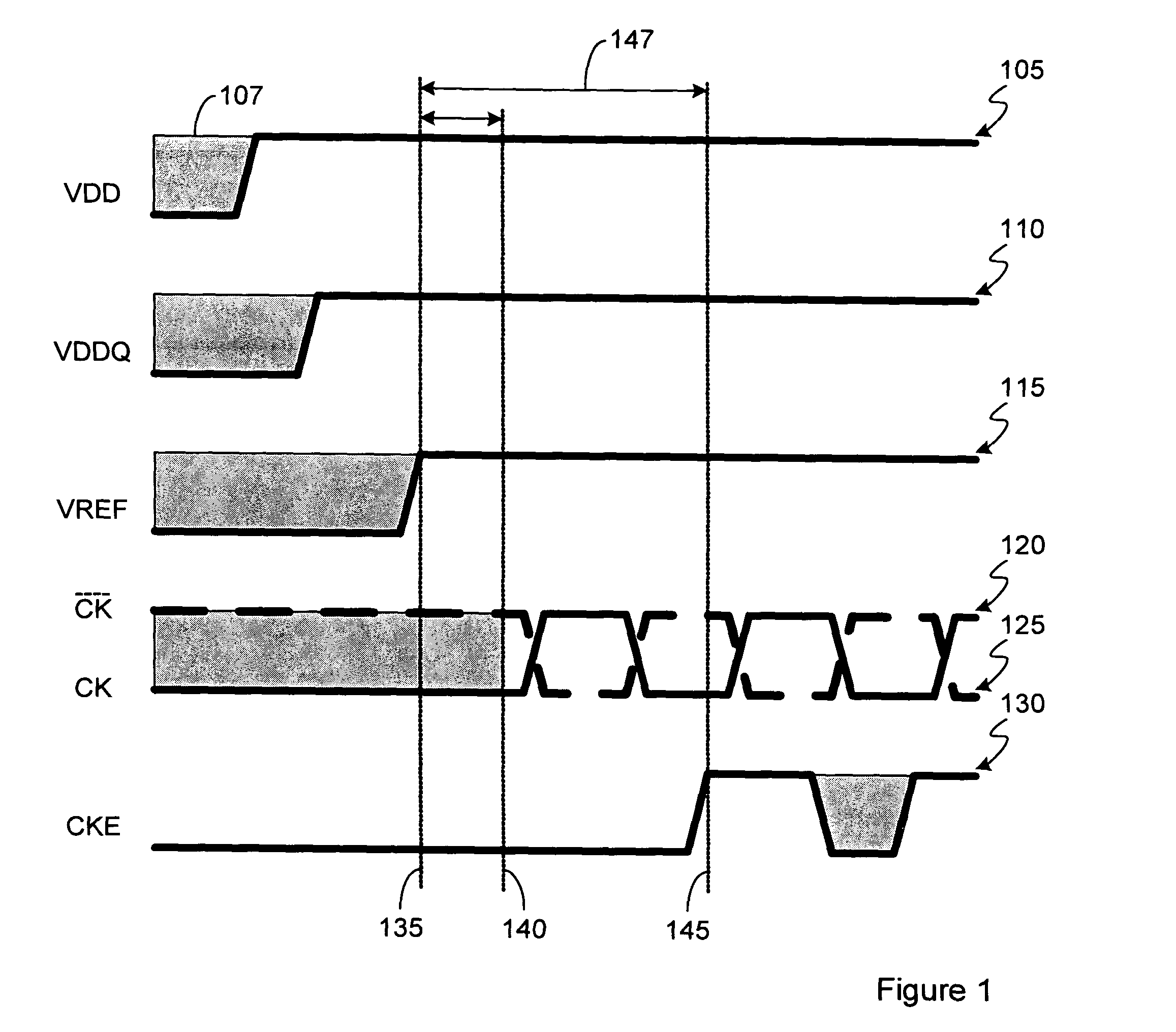
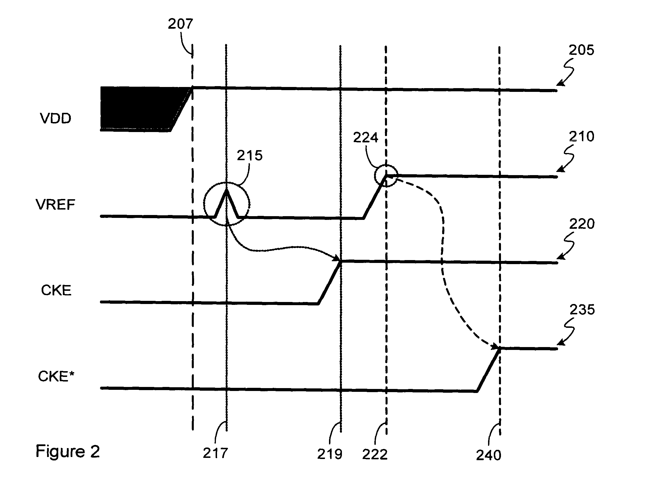
[0022] The present invention will be described with respect to preferred embodiments in a specific context, namely a memory adherent to the JEDEC DDR SDRAM technical standard. The JEDEC DDR SDRAM technical standard is published in a document entitled “JEDEC Standard—Double Data Rate (DDR) SDRAM Specification—JESD79C (Revision of JESD79B),” published March 2003, which is herein included by reference. The invention may also be applied, however, to other memories and integrated circuits wherein the accurate detection of a reference voltage signal during a power-on sequence is ...


PUM


Abstract

System and method for detecting a reference signal. A preferred embodiment comprises a latch (such as the latch 320) and a filter (such as the filter 325). The latch tracks a reference signal at its input and reflects the reference signal at its output. The filter can be coupled to the output of the latch and may inject a delay to help eliminate the effects of glitches and noise. When the reference signal reaches a specified value, a control signal from the filter causes the latch to store the reference signal. A delay imparted by the filter ensures that the latch does not store the reference signal until a finite amount of time after the reference signal reaches the specified value.

Description

TECHNICAL FIELD [0001] The present invention relates generally to a circuit for electronic circuit operation, and more particularly to a circuit for detecting a reference signal needed during a power-on sequence. BACKGROUND [0002] In a memory, differential signaling is typically used to transmit signals. Differential amplifiers can be used to compare differential inputs against a reference voltage signal to determine the value of a piece of data stored in a memory element, for example. It is therefore, important to have the reference voltage signal at the proper value prior to use. If the reference voltage signal is not at the proper value, then the comparisons made with the differential inputs can result in erroneous assignment of data stored in memory elements. [0003] According to the Joint Electronic Devices Engineering Council (JEDEC) technical standard for double data-rate synchronous dynamic random access memory (DDR SDRAM), inputs to the DDR SDRAM (“memory”), with the excepti...

Claims


Application Information

Patent Timeline
IPC IPC(8): H03K5/1252H03K17/22
CPCH03K17/223H03K5/1252
Inventor STREIF, HARALDKIEHL, OLIVERKILLIAN, MIKE
Owner POLARIS INNOVATIONS
Why Eureka
Try Eureka