Interference display cell and fabrication method thereof

a technology of optical interference display and manufacturing method, which is applied in the direction of instruments, transportation items, vehicle maintenance, etc., can solve the problems of worse resolution and the inability to avoid the wrong color of the optical interference display unit, and achieves simple and easy manufacturing process, high yield, and high quality.

Inactive Publication Date: 2005-03-03
SNAPTRACK
View PDF98 Cites 323 Cited by
  • Summary
  • Abstract
  • Description
  • Claims
  • Application Information

AI Technical Summary

Benefits of technology

[0012] It is therefore an objective of the present invention to provide a method for manufacturing an optical interference display unit structure, which method is suitable for manufacturing a color optical interference display with high resolution.
[0013] It is another an objective of the present invention to provide a method for manufacturing an optical interference display unit structure, which method is suitable for manufacturing an optical interference display with a simple and easy manufacturing process and high yield.
[0014] It is still another objective of the present invention to provide a method for manufacturing an optical interference display unit structure, which method is suitable for manufacturing optical interference display units where the support structure of the optical interference display unit is not damaged or removed in the process, and which is used to remove the photoresist layer and provide a high quality optical interference display plate.
[0015] In accordance with the foregoing objectives of the present invention, one preferred embodiment of the invention provides a method for manufacturing an optical interference display unit structure. The method for manufacturing an optical interference display unit structure disclosed in the present invention protects the support structure from damage or removal by the process, which is used to remove the photoresist layer on the second electrode. The method of fabricating the optical interference display unit structure is to form sequentially a first electrode and a sacrificial layer on a transparent substrate, and then form openings in the first electrode and the sacrificial layer. The openings are suitable for forming posts and support structure therein. Next, a photoresist layer is spin-coated on the sacrificial layer and fills the opening. A photolithographic process patterns the photoresist layer to define a post and the support structure.
[0019] In accordance with the method for manufacturing an optical interference display unit structure in present invention, at least two material layers are used to form the second electrode. The material layer located on the upper position is used to transfer the pattern of the photoresist layer thereon and the other material layers are used to protect the support structure from damage in the process for stripping the patterned photoresist layer. Concurrently, an optical interference display plate with high quality is produced. Therefore, the present invention discloses a method for manufacturing an optical interference display with a simple and easy manufacturing process and high yield.

Problems solved by technology

Therefore, the disadvantages of a worse resolution and wrong color of the optical interference display unit can't be avoided.

Method used


Image

  • Interference display cell and fabrication method thereof
  • Interference display cell and fabrication method thereof
  • Interference display cell and fabrication method thereof

Examples


embodiment

[0029] Embodiment

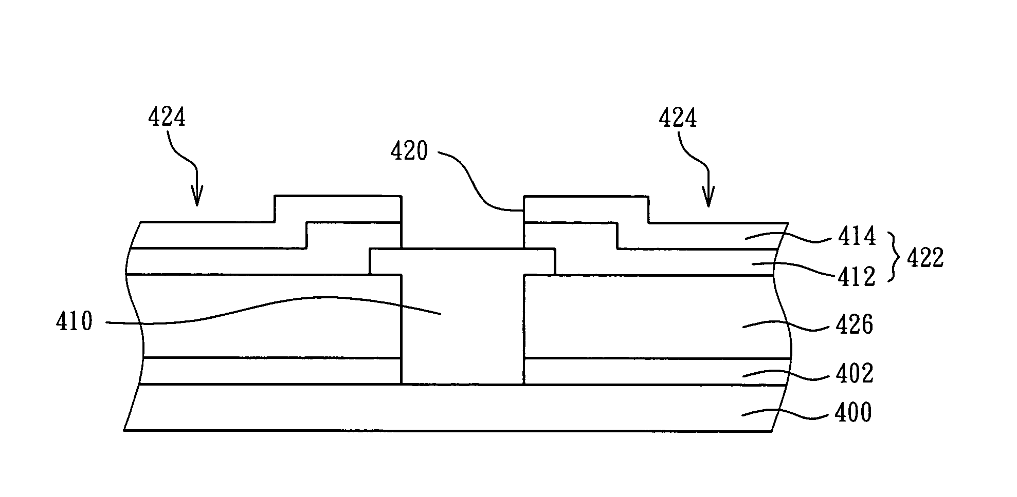
[0030]FIGS. 4A to 4D depict a method for manufacturing an optical interference display unit according to a preferred embodiment of the invention. Reference is made to FIG. 4A first, in which a first electrode 402 and a sacrificial layer 404 are formed in order on a transparent substrate 400. The sacrificial layer 404 is made of transparent materials such as dielectric materials, or opaque materials such as metal materials. Opening 406 is formed in the first electrode 402 and the sacrificial layer 404 by a photolithographic etching process. The opening 406 is suitable for forming a support structure therein. The transparent substrate 400 is, for example, a glass substrate and the first electrode 402 comprises at least one conductive transparent material layer. The conductive transparent material is indium tin oxide (ITO), indium zinc oxide (IZO), or indium oxide (IO).

[0031] Next, a material layer 408 is formed on the sacrificial layer 404 and fills the opening 406. ...


PUM


Abstract

An optical interference display unit with a first electrode, a second electrode and support structures located between the two electrodes is provided. The second electrode has at least a first material layer and a second material layer. At least one material layer of the two is made from conductive material and the second conductive layer is used as a mask while an etching process is performed to etch the first material layer to define the second electrode.

Description

FIELD OF INVENTION [0001] The present invention relates to a method for manufacturing an optical interference display. More particularly, the present invention relates to a method for manufacturing an optical interference display with posts of arms. BACKGROUND OF THE INVENTION [0002] Planar displays are popular for portable displays and displays with space limits because they are light and small in size. To date, planar displays in addition to liquid crystal displays (LCD), organic electro-luminescent displays (OLED), plasma display panels (PDP) and so on, as well as a mode of the optical interference display are of interest. [0003] U.S. Pat. No. 5,835,255 discloses an array of display units of visible light that can be used in a planar display. Reference is made to FIG. 1, which depicts a top view of a light interference display unit disclosed in the prior art. A plurality of first electrodes 102 is located in parallel on a substrate 100. A plurality of the second electrodes 104 is...

Claims


Application Information

Patent Timeline
Patent Type & Authority Applications(United States)
IPC IPC(8): G02B26/00
CPCG02B26/001E21D9/1093B60P3/062B60P1/16B60S9/10
Inventor LIN, WEN-JIAN
Owner SNAPTRACK
Why Eureka
Try Eureka