Wireless communication apparatus
- Summary
- Abstract
- Description
- Claims
- Application Information
AI Technical Summary
Benefits of technology
Problems solved by technology
Method used
Image
Examples
first embodiment
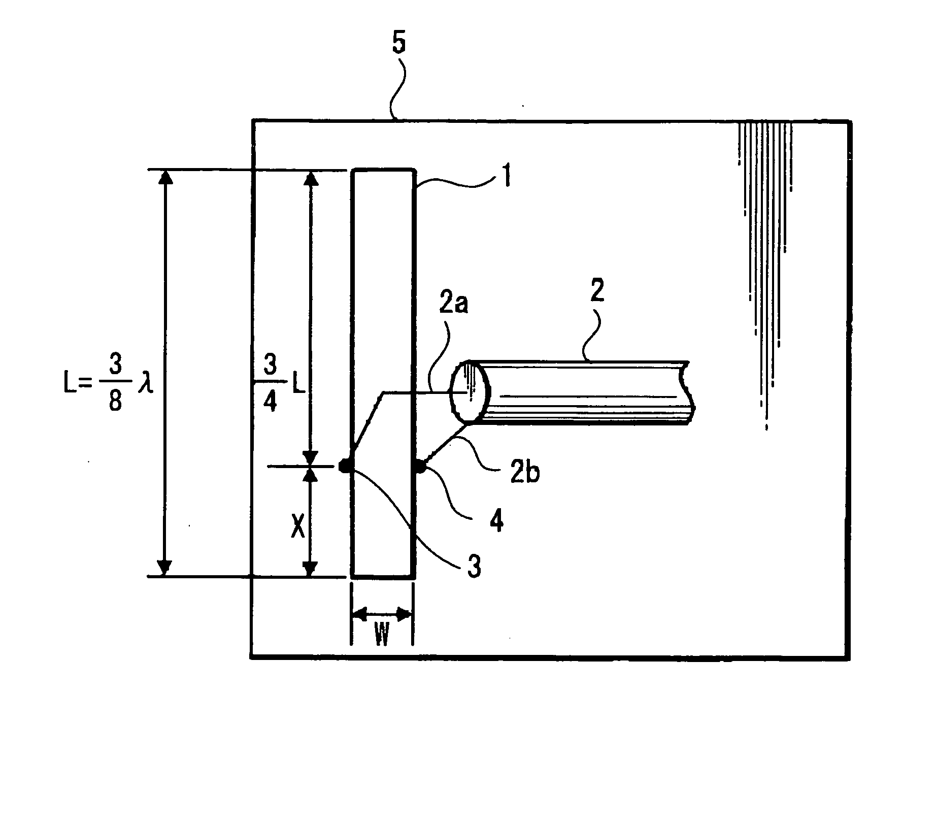
[0027]FIG. 2 shows an example of structure of an antenna device according to the present invention. As shown in FIG. 2, to obtain the wireless communication function of ISM band (2.4 GHz), a rectangular slit (opening) 1 having the length of 46.9 mm that is equal to ⅜λ is provided in a metal plate 5 on the surface of a metal housing, and a feeder 2 is connected to a feeding point 3 located on the metal portion at the position approximately three-quarters of the long side L of the slit 1. The feeder 2 is connected to a transmitter or a receiver, which is not shown in a drawing and is located inside the housing. As the feeder 2, an unbalanced transmission line may be used, and in this example, a coaxial cable is used. Hereupon, a core wire conductor of a signal line 2a of the coaxial cable is connected to a feeding point 3, and an external sheath conductor of a ground line 2b is connected to a ground point 4 located at the metal portion on the opposite side of the feeding point 3 locat...
second embodiment
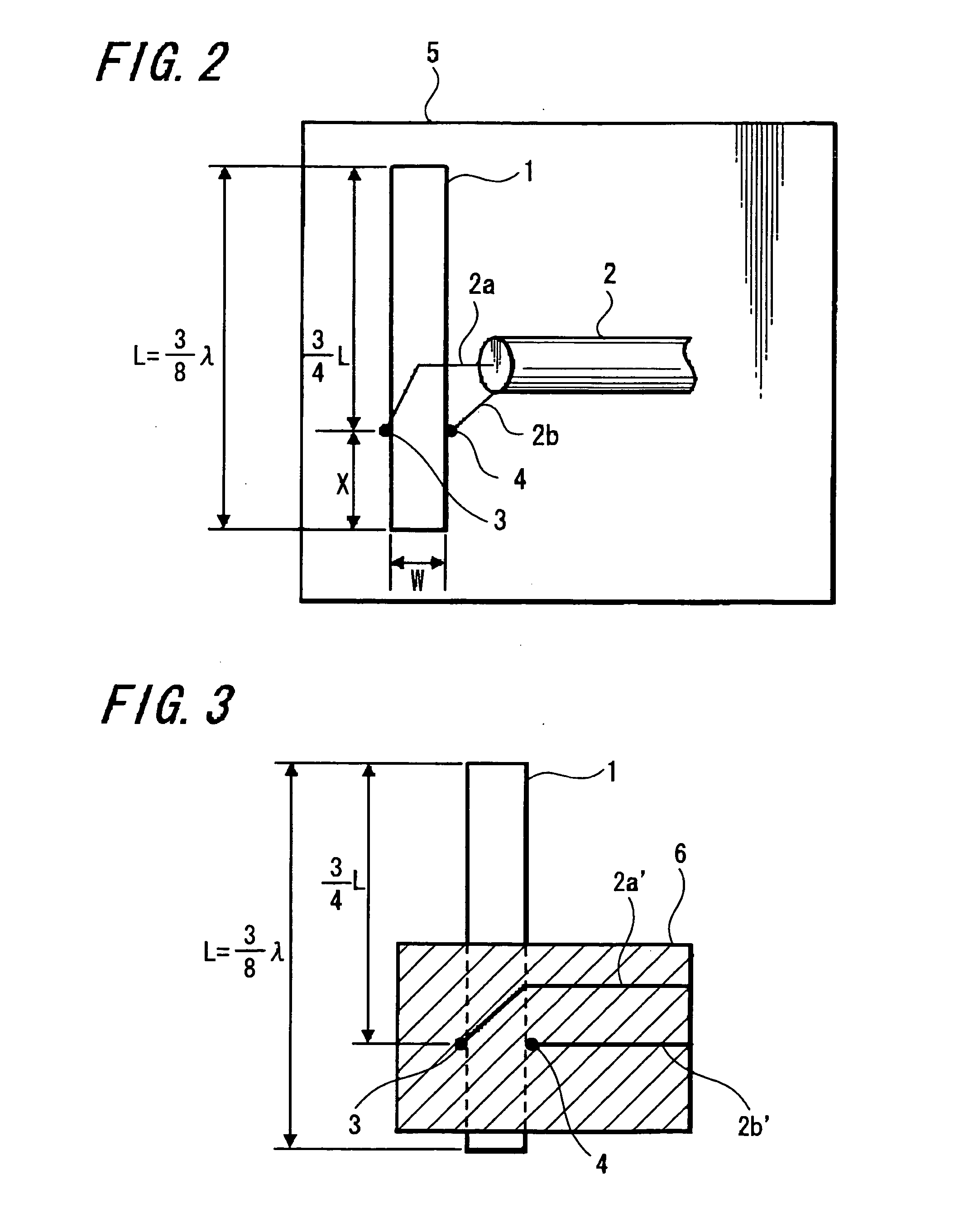
[0028]FIG. 3 shows an example of structure of an antenna device according to the present invention. In FIG. 3, a rectangular slit (opening) 1 having the length of 46.9 mm that is equal to ⅜λ is also provided in the metal plate on the surface of the metal housing, and a feeder is connected to a feeding point 3 located on the metal portion at the position approximately three-quarters of the long side of the slit 1. In this example, a feeder is constructed using a microstrip line on a PCB (Printed Circuit Board) 6. The microstrip line is also an unbalanced transmission line, and here a transmission line 2a′ of the microstrip line is connected to the feeding point 3, and a conduction portion 2b′ constituting a ground plane is connected to a ground point 4.
[0029] Note that the width of the slit 1 explained in the first and second embodiments, namely the width W of slit 1 shown in FIG. 2, can be adjusted in accordance of the band width to be used. The broader the width W becomes, the more...
third embodiment
[0034] Next, an example of structure of an antenna device according to the present invention is shown in FIG. 6. In FIG. 6, a slit 12 is provided in the metal plate on the surface of a metal housing, and a feeder 2 is connected to a feeding point 3 located on the metal portion at the position approximately ¾ of the long side L′ of the slit 12. Further, the opening of the slit 12 is filled with a dielectric material 8 such as plastics or others. Accordingly, as shown in the following Formula 1, by filling the opening of slit 12 with the dielectric material 8, the length L′ of the slit can be made short depending upon the value of an effective relative dielectric coefficient of this slit 12. [Formula 1]L′=3λ8ɛ eff
[0035] For example, when the slit 12 is filled with ABS resin (Acrylonitrile Butadiene styrene resin) and in the case where an effective dielectric coefficient of the slit portion is εeff=4, the length L′ of the slit 12 becomes ½ of the length 46.9 mm of the slit explaine...
PUM
 Abstract
Description
Claims
Application Information


