Cutting cam peak power by clock regioning

a clock region and cam technology, applied in the field of cam peak power reduction, can solve the problems of cam device b>200/b> having a peak power consumption which may be significantly higher, cam device b>200/b> having a significantly higher peak power consumption, etc., and achieve the effect of reducing the peak power consumption of the cam devi

Inactive Publication Date: 2005-03-10
MICRON TECH INC
View PDF3 Cites 9 Cited by
  • Summary
  • Abstract
  • Description
  • Claims
  • Application Information

AI Technical Summary

Benefits of technology

[0013] The invention provides a CAM device architecture where the CAM cells are divided into at least two arrays. Each array is operated in a different clock domain so that each array is prevented from drawing maximum power at a same time. By dividing the CAM array into a plurality of arrays and staggering the search operation so that every array does not simultaneously draw maximum power, the peak power consumption of the CAM device is reduced.

Problems solved by technology

However, CAM devices 200 consume significantly more power and produce significantly more switching noise than a conventional memory device, especially during a first portion of the search operation because the CAM cells 100 are accessed and searched simultaneously.
This results in the CAM device 200 having a peak power consumption which may be significantly higher than the average power consumption during a portion of each match operation.
The high peak power consumption requires the CAM device 200 to be used with a robust power supply, and also increases heat production.

Method used


Image

  • Cutting cam peak power by clock regioning
  • Cutting cam peak power by clock regioning
  • Cutting cam peak power by clock regioning

Examples


Embodiment Construction

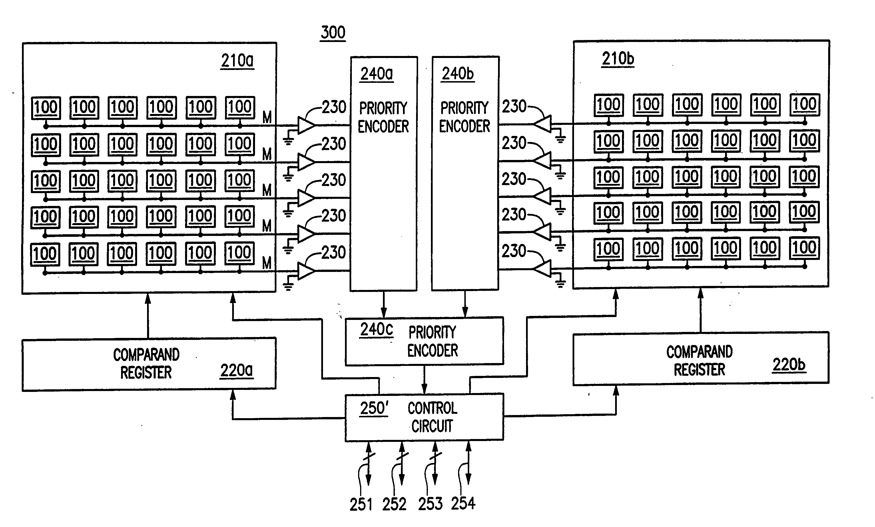
[0023] Now referring to the drawings, where like reference numerals designate like elements, there is shown in FIG. 3A a block diagram of a CAM device 300 constructed in accordance with a first exemplary embodiment of the invention. The CAM cells 100 of device 300 are organized into two arrays 210a, 210b. As illustrated, the two arrays 210a, 210b respectively are oriented left and right of encoders 240a, 240b. However, it should be understood that the orientation of the two arrays 210a, 210b may be varied without departing from the scope of the invention. As illustrated, each array 210a, 210b is associated with a respective comparand register 220a, 220b. However, it should be understood that a single comparand register coupled to both arrays 210a, 210b may also be used without departing from the scope of the invention. Each row of CAM cells 100 is coupled to a respective match line M. Each match line M couples its row to a priority encoder 240a, 240b via a respective sense amplifier...


PUM


Abstract

A CAM device architecture where CAM cells are divided into at least two arrays and each array is operated in a different clock domain so that at no time are the arrays simultaneously drawing maximum power. By dividing the CAM array into a plurality of arrays and staggering the search operation so that every array does not simultaneously draw maximum power, the peak power consumption of the CAM device is reduced.

Description

[0001] This application is a continuation of applicatoin Ser. No. 10 / 655,215, filed Sep. 5, 2003, the subject matter of which is incorpoated by reference herein.FIELD OF INVENTION [0002] The present invention relates generally to semiconductor memory devices and, more particularly to peak power reduction in content addressable memory (CAM) devices. BACKGROUND OF THE INVENTION [0003] An essential semiconductor device is semiconductor memory, such as a random access memory (RAM) device. A RAM allows a memory circuit to execute both read and write operations on its memory cells. Typical examples of RAM devices include dynamic random access memory (DRAM) and static random access memory (SRAM). [0004] Another form of memory is the content addressable memory (CAM) device. A CAM is a memory device that accelerates any application requiring fast searches of a database, list, or pattern, such as in database machines, image or voice recognition, or computer and communication networks. CAMs pr...

Claims


Application Information

Patent Timeline
Patent Type & Authority Applications(United States)
IPC IPC(8): G11C15/00
CPCG11C15/00
Inventor RADKE, WILLIAM
Owner MICRON TECH INC
Why Eureka
Try Eureka