Method of manufacturing luminescence device, and luminescence device

a luminescence device and luminescence technology, applied in the direction of coatings, printing, electroluminescent light sources, etc., can solve the problems of reducing the manufacturing cost, deteriorating the luminescence characteristic, and remarkably waste of resin materials, and achieve the effect of long lasting and less costly

Inactive Publication Date: 2005-03-10
SEIKO EPSON CORP
View PDF14 Cites 35 Cited by
  • Summary
  • Abstract
  • Description
  • Claims
  • Application Information

AI Technical Summary

Benefits of technology

[0019] Next, the luminescence device according to the invention is obtained by the above-described manufacturing method. According to such luminescence device, because it is difficult for the second electrode and the function lay

Problems solved by technology

However, in these methods, the resin material is remarkably wasted, thereby causing a big problem in reducing the manufacturing cost.
H5-36475 proposes a method of covering with a protective layer, made of a high molecular compound with electrical insulating property, such as a vacuum deposition method, a sputtering method, a CVD method, however, for example, in the sputtering method, damage is given to the luminescence layer, and thus the luminescence characteristic deteriorates.
Also, in the CVD method, t

Method used


Image

  • Method of manufacturing luminescence device, and luminescence device
  • Method of manufacturing luminescence device, and luminescence device
  • Method of manufacturing luminescence device, and luminescence device

Examples


Embodiment Construction

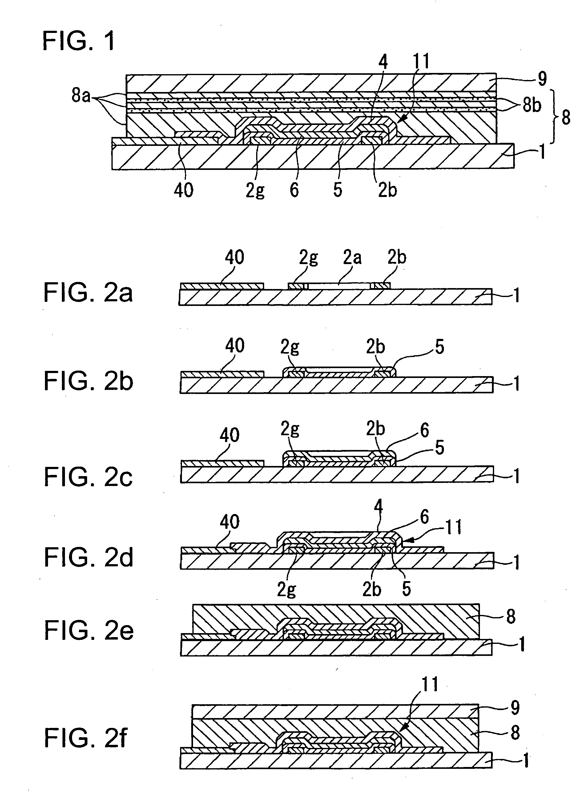
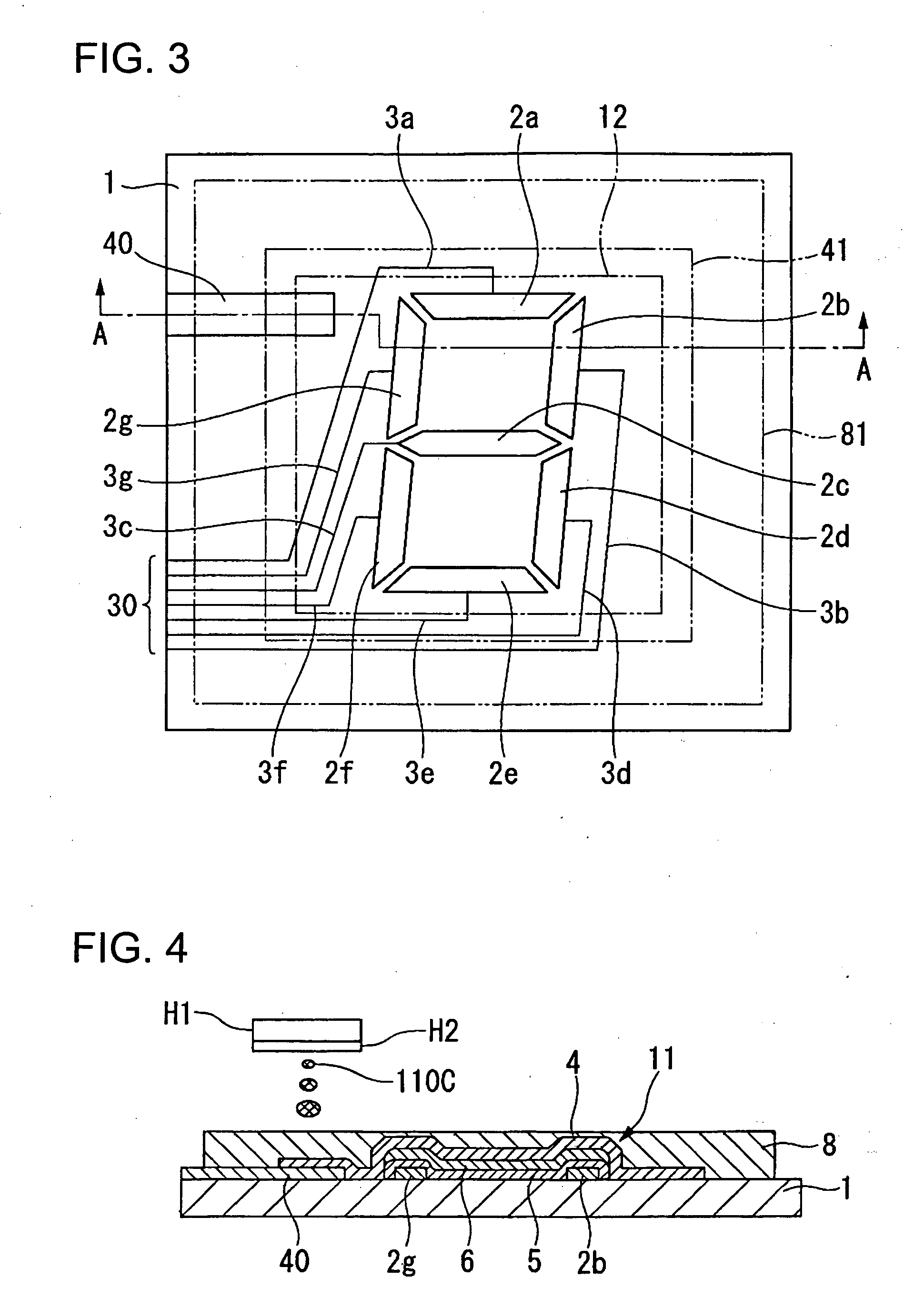
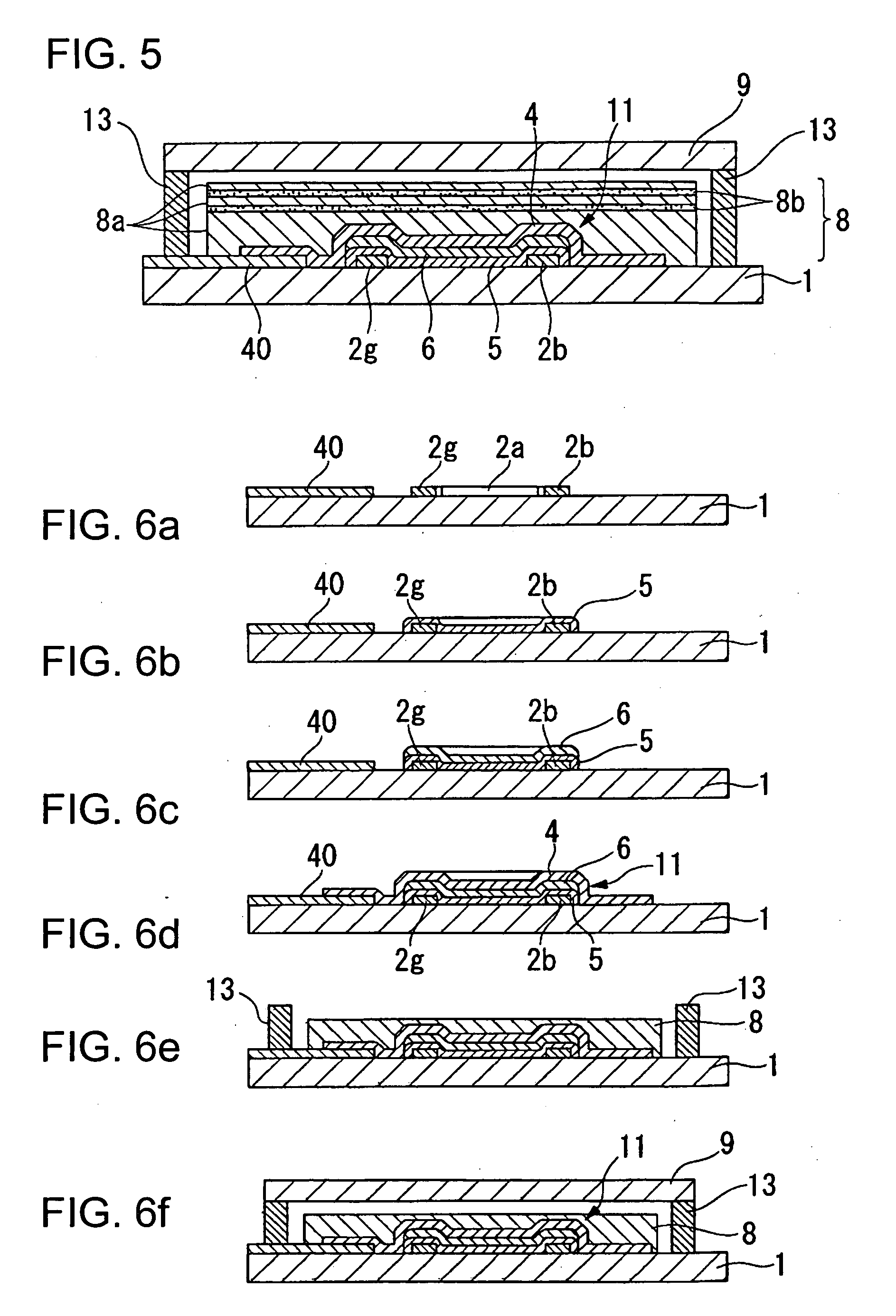
[0032] Hereinafter, exemplary embodiments according to the invention will be described with reference to drawings. A first exemplary embodiment of an organic electro-luminescence device, which is one example of a luminescence device according to the present invention, will be described by referring to FIGS. 1 through 3. FIG. 1 is a view showing a structure of the organic electro-luminescence device, and is a cross-sectional view corresponding to a cross section along the A-A line of FIG. 3. FIG. 2 is a cross-sectional view showing each step of a method of manufacturing the organic electro-luminescence device. FIG. 3 is a plan view showing one condition of the manufacturing process of the organic electro-luminescence device, and shows the condition of FIG. 2(a).

[0033] The organic electro-luminescence device of the exemplary embodiment can include seven elements, which constitute a digital number, as a luminescence portion formed of organic electro-luminescence elements. The organic ...


PUM


Abstract

Aspects of the invention provide a method of manufacturing a luminescence device including forming the first electrode on a substrate, forming a function layer including a luminescence layer on the first electrode, forming a second electrode on the function layer, and forming a sealing layer that covers a luminescence portion, formed of the first electrode, the function layer, and the second electrode, and the sealing layer is formed by an ink-jet method. Accordingly, the deterioration of a luminescence device that is sealed with the sealing layer can be prevented for a long period of time by an inexpensive method.

Description

BACKGROUND OF THE INVENTION [0001] 1. Field of Invention [0002] The invention relates to a method of manufacturing a luminescence device, and in particular to a technology of sealing a substrate of the luminescence device. [0003] 2. Description of Related Art [0004] In recent years, development of an organic electro-luminescence device (a luminescence device with a structure having a luminescence layer, made of organic material, between an anode and a cathode) as a self-luminescence type display in place of a liquid crystal display has been progressing rapidly. As for a structure of an organic electro-luminescence device, for example, a stacked structure, where an anode formed of a transparent electrode, a positive hole injection / transportation layer, a luminescence layer formed of organic material, and a cathode having no optical transparency are formed on a transparent substrate in this order, is cited. In the organic electro-luminescence device with this stacked structure, light ...

Claims


Application Information

Patent Timeline
IPC IPC(8): H01L51/00H05B33/04H01L51/50H01L51/52H05B33/10H05B33/14
CPCH01L51/5237H01L51/0005H10K71/135H10K50/8445H10K50/841
Inventor ISHIDA, KOHEI
Owner SEIKO EPSON CORP
Why Eureka
Try Eureka