Techniques for patterning features in semiconductor devices

a technology of semiconductor devices and features, applied in semiconductor devices, thin material processing, electrical equipment, etc., can solve the problems of large variations in critical dimensions across the board, difficult control of resist reflow, and reduced critical dimensions of patterned features

Inactive Publication Date: 2005-03-17
GLOBALFOUNDRIES US INC
View PDF9 Cites 19 Cited by
  • Summary
  • Abstract
  • Description
  • Claims
  • Application Information

AI Technical Summary

Benefits of technology

[0006] The present invention provides techniques for semiconductor processing. In one aspect of the invention, a method for patterning one or more features in a semiconductor device comprises the following step. At least one critical dimension of the one or more features is reduced during etching of the antireflective material.

Problems solved by technology

Conventional techniques to reduce the critical dimensions of patterned features exist, however, these techniques have several drawbacks.
Resist reflow is extremely difficult to control because very small temperature variations across the bake plate can cause large variations in the critical dimensions across each wafer.
This technique, being highly specific to the resist type, is difficult to implement.
Moreover, the crosslinked overcoat film offers poor etch resistance during the substrate etch step, thus, negating any reductions in critical dimensions obtained.
Silylating resists can also be used to chemically bias resist features, but they also suffer from cross-wafer and nested-isolated bias issues.
The above techniques may further result in features having corners that are not sharp, but rounded.
If the critical dimensions of the feature top is too large to begin with, the effectiveness of this technique is at best very limited.

Method used


Image

  • Techniques for patterning features in semiconductor devices
  • Techniques for patterning features in semiconductor devices
  • Techniques for patterning features in semiconductor devices

Examples


Embodiment Construction

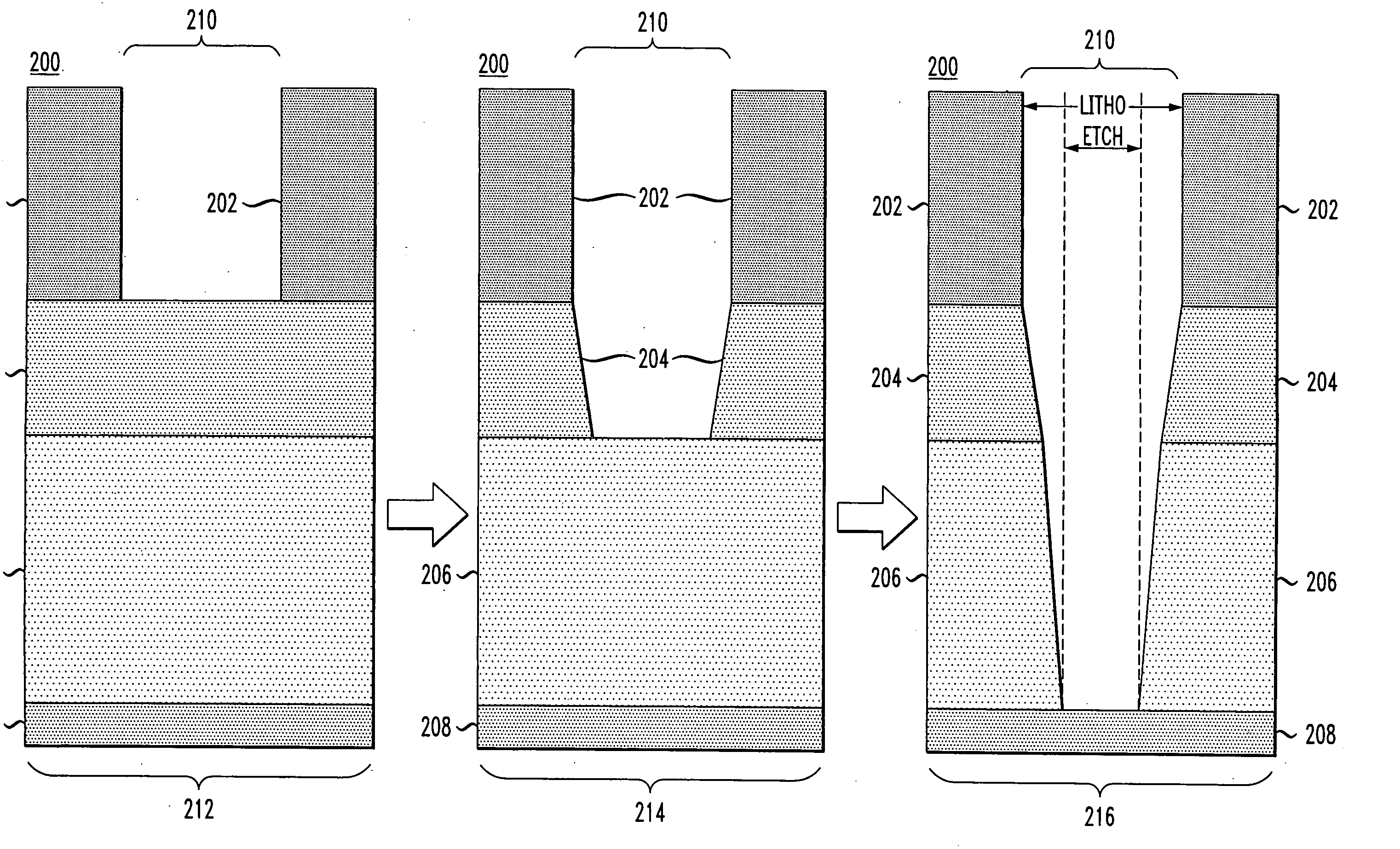
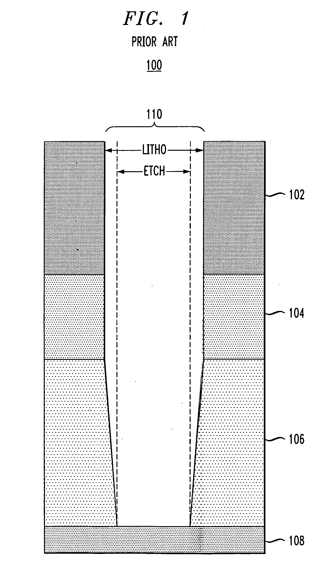
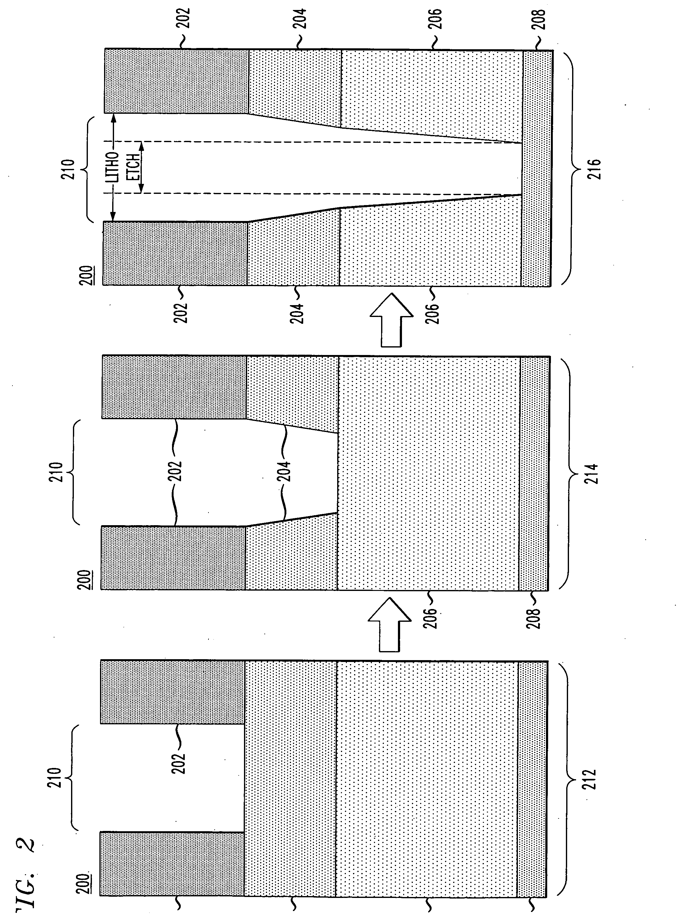
[0013]FIG. 1 is a diagram illustrating a semiconductor device with a feature having reduced critical dimensions etched therein using conventional techniques. As shown in FIG. 1, semiconductor device 100 comprises radiation sensitive imaging layer 102 deposited on antireflective material 104. Antireflective material 104 is deposited on substrate 106. Substrate 106 is deposited on nitride layer 108. Feature 110 is etched into radiation sensitive imaging layer 102, antireflective material 104 and substrate 106.

[0014] According to conventional methods for reducing the critical dimensions of etched features in semiconductor devices, the critical dimensions of feature 110 are changed, i.e., reduced, solely in substrate 106. As such, the critical dimensions of feature 110 remain unchanged during the etching of radiation sensitive imaging layer 102 and antireflective material 104. Reduction of the critical dimensions of feature 110 in radiation sensitive imaging layer 102 or antireflective...


PUM


Abstract

Techniques for semiconductor processing are provided. In one aspect, a method for patterning one or more features in a semiconductor device comprises the following step. At least one critical dimension of the one or more features is reduced during etching of the antireflective material. A lithographic structure is also provided.

Description

FIELD OF THE INVENTION [0001] The present invention relates to semiconductor processing and, more particularly, to reducing critical dimensions of features patterned in a semiconductor device. BACKGROUND OF THE INVENTION [0002] Technology often demands the patterning of features smaller than those lithographically possible. For example, while patterning features, such as contact holes and vias, it may be desirable to have features with critical dimensions defined in the substrate that are smaller than lithographically defined in the resist. The critical dimensions of a feature comprise the characteristic dimensions of the feature attained by the technology employed. Conventional techniques to reduce the critical dimensions of patterned features exist, however, these techniques have several drawbacks. [0003] One common technique to reduce the critical dimensions includes the use of resist reflow and overcoat films, e.g., resolution enhancement lithography assisted by chemical shrink ...

Claims


Application Information

Patent Timeline
Patent Type & Authority Applications(United States)
IPC IPC(8): H01L21/027H01L21/033H01L21/311
CPCH01L21/0276H01L21/0337H01L21/0338Y10T428/24802H01L21/31144Y10T428/24926H01L21/31116B82Y40/00
Inventor ALLEN, SCOTT D.BABICH, KATHERINA E.HOLMES, STEVEN J.MAHOROWALA, ARPAN P.PFEIFFER, DIRKWISE, RICHARD STEPHAN
Owner GLOBALFOUNDRIES US INC
Why Eureka
Try Eureka