Thin film transistor with self-aligned intra-gate electrode
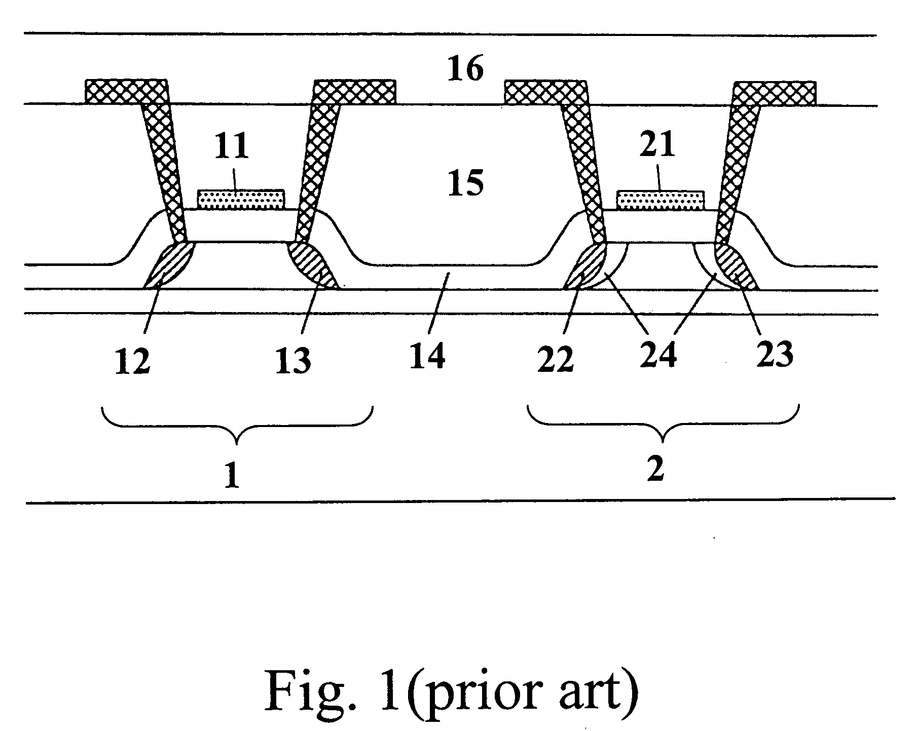
a thin film transistor and intra-gate electrode technology, applied in the field of thin film transistors, can solve the problems of low response speed, photo-misalignment problem, and restricted application, and achieve the effect of reducing the problem of photo-misalignmen
- Summary
- Abstract
- Description
- Claims
- Application Information
AI Technical Summary
Benefits of technology
Problems solved by technology
Method used
Image
Examples
first embodiment
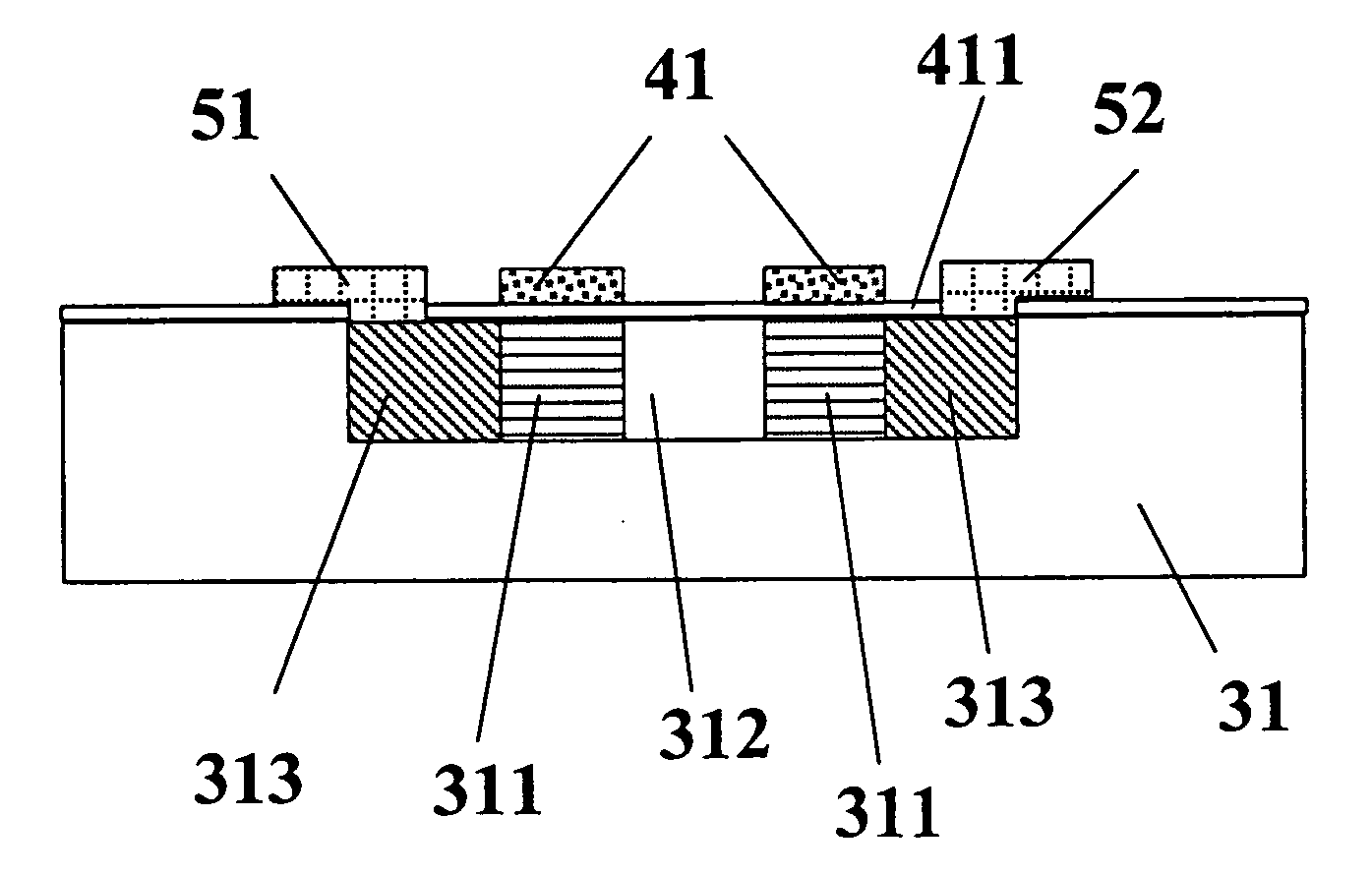
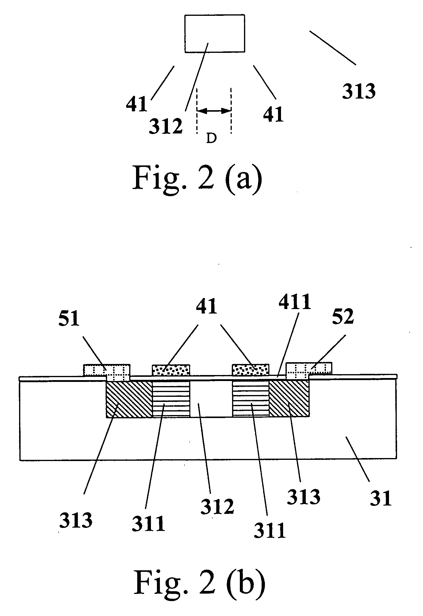
[0029] FIGS. 2(a) and 2(b) are top view and cross-sectional view illustrating a thin film transistor for use in an active matrix liquid crystal display according to the present invention, respectively. The thin film transistor of the present invention comprises a substrate 31. In the substrate 31, there is provided a plurality of intrinsic regions 311, at least one first doped region 312 (which can be n-doped regions) and two second doped regions 313. The first doped region 312 is disposed between the intrinsic regions 311. The intrinsic regions 311 are linked together to form a connection structure via the first doped region 311. The two second doped regions 313 are disposed at both ends of the connection structure, respectively. Furthermore, this thin film transistor further comprises a source region 51 and a drain region 52, which are coupled to the two second doped regions 313 disposed at both ends of the connection structure, respectively. This thin film transistor further comp...
second embodiment
[0031] FIGS. 3(a) and 3(b) are schematic views illustrating a thin film transistor according to the present invention. In FIG. 3(a), the relative locations of the intrinsic regions 311, the first doped region 312 and the second doped regions 313 are shown. The intrinsic regions 311, the first doped region 312 and the second doped regions 313 are arranged in an inverse L-shaped configuration. In other words, the first doped region 312 comprises two portions in vertical arrangement to each other. The intrinsic regions 311 are linked together to form a connection structure via the first doped region 311. The two second doped regions 313 are disposed at both ends of the connection structure, respectively. Furthermore, this thin film transistor further comprises a source region and a drain region (not shown), which are coupled to the two second doped regions 313 disposed at both ends of the connection structure, respectively. In FIG. 3(b), the gate electrode 41 is arranged in an L-shaped...
third embodiment
[0032] the present invention can be seen in FIGS. 4(a) and 4(b). In FIG. 4(a), the relative locations of the intrinsic regions 311, the first doped region 312 and the second doped regions 313 are shown. The intrinsic regions 311, the first doped region 312 and the second doped regions 313 are arranged in approximately a U-shaped configuration. In other words, the first doped region 312 is arranged in approximately a U-shaped configuration. The intrinsic regions 311 are linked together to form a connection structure via the first doped region 311. The two second doped regions 313 are disposed at both ends of the connection structure, respectively. Furthermore, this thin film transistor further comprises a source region and a drain region (not shown), which are coupled to the two second doped regions 313 disposed at both ends of the connection structure, respectively. In FIG. 4(b), the gate electrode 41 is arranged in an I-shaped configuration and disposed over the intrinsic regions 3...
PUM
 Abstract
Description
Claims
Application Information


