Bumped wafer with adhesive layer encompassing bumps and manufacturing method thereof
- Summary
- Abstract
- Description
- Claims
- Application Information
AI Technical Summary
Benefits of technology
Problems solved by technology
Method used
Image

Examples
Embodiment Construction
[0017] The bumped wafer package and the manufacturing method thereof according to the preferred embodiment of this invention will be described herein below with reference to the accompanying drawings, wherein the same reference numbers are used in the drawings and the description to refer to the same or like parts.
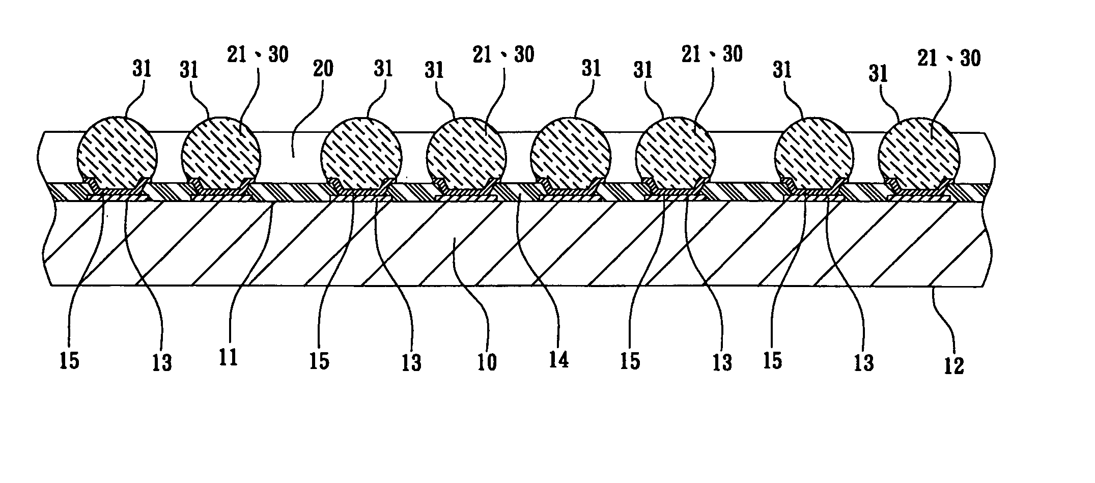
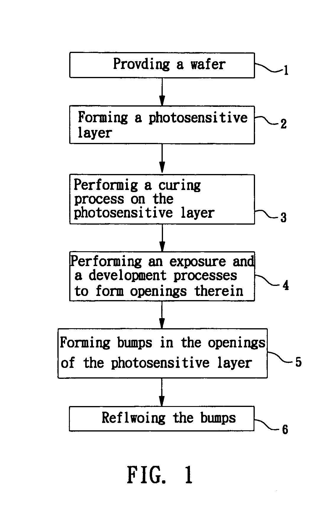
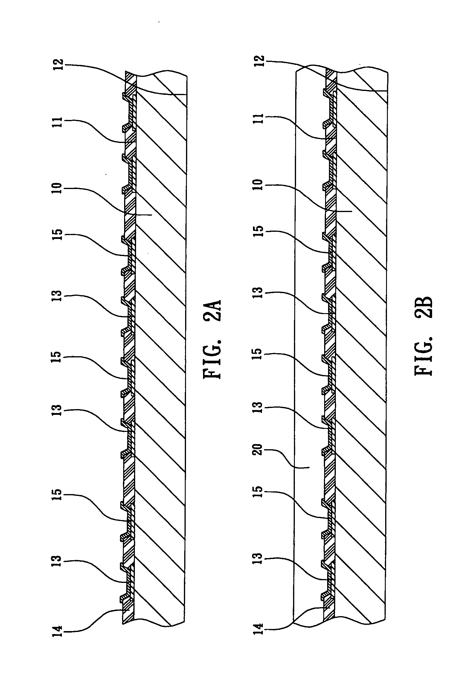
[0018] As shown in FIG. 1, it illustrates a process flow of a manufacturing method of the bumped wafer package. The manufacturing method mainly comprises the following steps of providing a wafer as shown in step 1, forming a photosensitive adhesion layer on the wafer as shown in step 2, curing the photosensitive adhesion layer as shown in step 3, performing exposure and development processes to form a plurality of openings in the photosensitive adhesion layer as shown in step 4, forming a plurality of bumps in the openings 5 and reflowing the bumps to shape the bumps into balls as shown in steps 5 and 6. Referring to FIG. 2A, it illustrates the step 1. Therein, the wafer ...
PUM
 Abstract
Description
Claims
Application Information
 - Generate Ideas
- Intellectual Property
- Life Sciences
- Materials
- Tech Scout
- Unparalleled Data Quality
- Higher Quality Content
- 60% Fewer Hallucinations
Browse by: Latest US Patents, China's latest patents, Technical Efficacy Thesaurus, Application Domain, Technology Topic, Popular Technical Reports.
© 2025 PatSnap. All rights reserved.Legal|Privacy policy|Modern Slavery Act Transparency Statement|Sitemap|About US| Contact US: help@patsnap.com