Semiconductor light-emitting device

a technology of semiconductors and light-emitting devices, which is applied in the direction of discharge tubes/lamp details, discharge tubes luminescnet screens, electric discharge lamps, etc., can solve the problems of reducing the amount of light, and deteriorating of fluorescent materials over tim

Inactive Publication Date: 2005-03-17
STANLEY ELECTRIC CO LTD
View PDF10 Cites 53 Cited by
  • Summary
  • Abstract
  • Description
  • Claims
  • Application Information

AI Technical Summary

Problems solved by technology

In such a case, the fluorescent material can deteriorate over time because it receives ultraviolet and visible lights contained in the light emitted from the LED chip and extraneous light such as sunlight.
As a result, some problems arise because the tone of the light emitted from the LED is shifted and the amount of the light is lowered.
However, there are not sufficient measures for ensuring the amount of light and for reducing the variation in tone.

Method used


Image

  • Semiconductor light-emitting device
  • Semiconductor light-emitting device
  • Semiconductor light-emitting device

Examples


embodiment

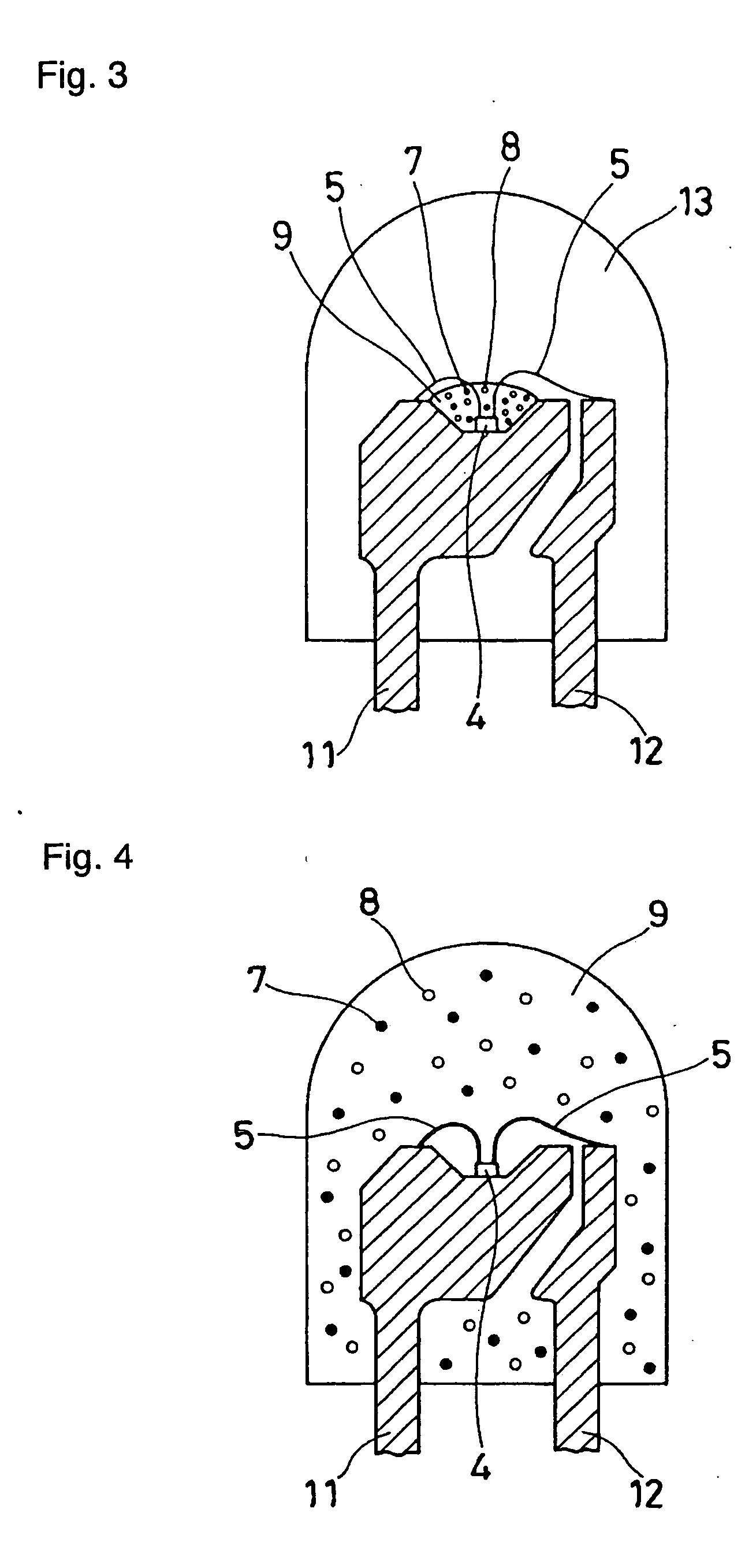
[0035] Embodiment of FIG. 4

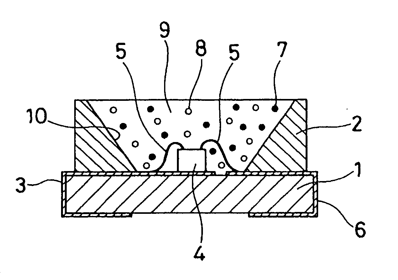
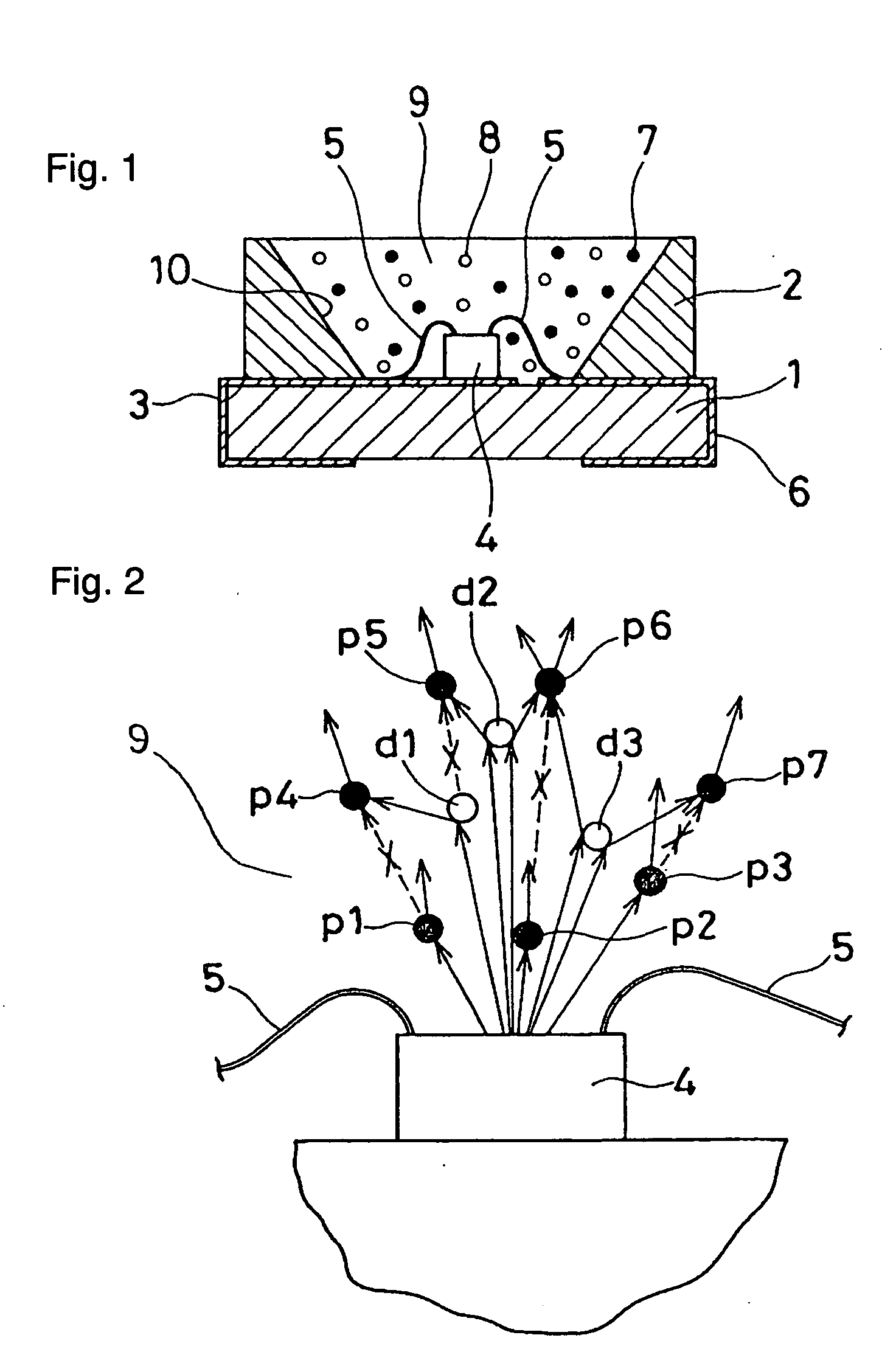
[0036]FIG. 4 is a cross-sectional view showing the structure of a semiconductor light-emitting device according to another embodiment of the present invention. The embodiment of FIG. 4 is also directed to a shell-type LED similar to the embodiment of FIG. 3 described above. At the tip of one of two lead frames 11, 12, a conical recess having a reflective inner side can be formed. An LED chip 4 is preferably mounted on the bottom in the recess. Two electrodes can be provided on the upper surface of the LED chip 4. One of the electrodes can be connected to the lead frame 11 via a bonding wire 5 to achieve electrical conduction therebetween. The other electrode can be connected to the lead frame 12 via a bonding wire 5 to achieve electrical conduction therebetween. The tip of the lead frame 11 with the LED chip 4 mounted thereon can be covered with a wavelength converter material 9, which preferably contains a fluorescent material 7 and a 20-80 wt. % diffuser...


PUM


Abstract

A semiconductor light-emitting device can serve as a high-brightness light source with less tone variation. A reflective frame having a conical recess can be provided on a substrate. An LED chip can be mounted on the bottom in the reflective frame. A wavelength converter material is preferably filled in the recess to seal the LED chip. The wavelength converter material can include a fluorescent material and a 20-80 wt. % diffuser mixed in an optically transmissive resin.

Description

[0001] This invention claims the benefit of Japanese patent application No. 2003-324884, filed on Sep. 17, 2003, which is hereby incorporated by reference. BACKGROUND OF THE INVENTION [0002] 1. Field of the Invention [0003] The present invention relates to a semiconductor light-emitting device. More particularly, it relates to a semiconductor light-emitting device operative to provide toned light through mixture of light emitted from a semiconductor light-emitting element (light-emitting diode chip) with light emitted from the light-emitting diode chip that is wavelength-converted at a fluorescent material in combination. [0004] 2. Description of the Related Art [0005] A light-emitting diode (LED) chip operative to emit a light having a sharp spectrum distribution characteristic can be employed as a light source to achieve an LED that emits a white light. In this case, the light emitted from the LED chip can be mixed with a wavelength-converted light emitted / caused by a fluorescent ...

Claims


Application Information

Patent Timeline
Patent Type & Authority Applications(United States)
IPC IPC(8): H01L33/50H01L33/54H01L33/56H01L33/60H01L33/62
CPCH01L33/56H01L2933/0091H01L2224/48091H01L2224/48247H01L2224/8592H01L2224/48257H01L2924/00014H01L2924/181
Inventor MORITA, YASUMASAOBA, HAYATOFUJISAWA, SHIGEOTANAKA, MINORU
Owner STANLEY ELECTRIC CO LTD
Why Eureka
Try Eureka