Connector sheet and wiring board, and production processes of the same

a technology of connecting wires and wiring boards, applied in the direction of electrical apparatus construction details, circuit inspection/indentification, printed circuit aspects, etc., to achieve the effect of narrowing a wiring pitch, high wiring density and rapid production

Inactive Publication Date: 2005-03-17
PANASONIC CORP
View PDF3 Cites 59 Cited by
  • Summary
  • Abstract
  • Description
  • Claims
  • Application Information

AI Technical Summary

Benefits of technology

Considering the above matters, the present inventions have been made, and one of the purposes thereof is to provide a connection element which allows the repair on the way of the connecting procedure and also which is adaptable to the narrow wiring pitch. Other purpose is to use such connection element so as to preferably at a low cost, produce a multi-layered wiring board or a module which contains wiring layers (or wiring patterns) with a high wiring density and fine wiring pitch. A further purpose is to provide processes for producing such connection element, such multi-layered wiring board and such module respectively.
In any of the connector sheets according to the present invention, one preferable embodiment thereof comprises a release film which is placed on at least one of the front surface and the rear surface of the sheet substrate. As a result thereof, the connector sheet may be readily handled. In other preferable embodiment, the connector sheet comprises in addition to or in place of the release film, a wiring layer (or a wiring pattern) which is placed on at least one of the front surface and the rear surface of the sheet substrate. When the connector sheet includes the both of the wiring layer and the release film on one or each side thereof, the release film forms the outermost layer.
In any of the connector sheets according to the present invention, the tackiness under the first condition may be reduced and preferably substantially disappear under a third condition of a temperature which is lower than the temperature of the second condition. That is, the peel strength as a measure of the tackiness which strength will be explained later becomes smaller and preferably greatly smaller relative to that under the first condition.
It is noted that the step (f) may be carried out under a third condition which comprises a temperature lower than the temperature of the first condition, whereby the tackiness is reduced, so that the separation becomes easier.
According to the present invention, when the connector sheet having the wiring layer is connected to a portion of a surface (or side) of the wiring board element, the multi-layered wiring board as a product wiring board can be readily produced which has a part where the number of wiring layers is larger compared with the other part, and the wiring layer(s) of the former part may have a high wiring density and narrow a wiring pitch. As a result, the product wiring board having the wiring layer(s) with the high wiring density and fine wiring pitch can be produced inexpensively.

Problems solved by technology

However, under the first condition, the curing reaction may occur, but it is never completed.

Method used


Image

  • Connector sheet and wiring board, and production processes of the same
  • Connector sheet and wiring board, and production processes of the same
  • Connector sheet and wiring board, and production processes of the same

Examples


embodiment 1

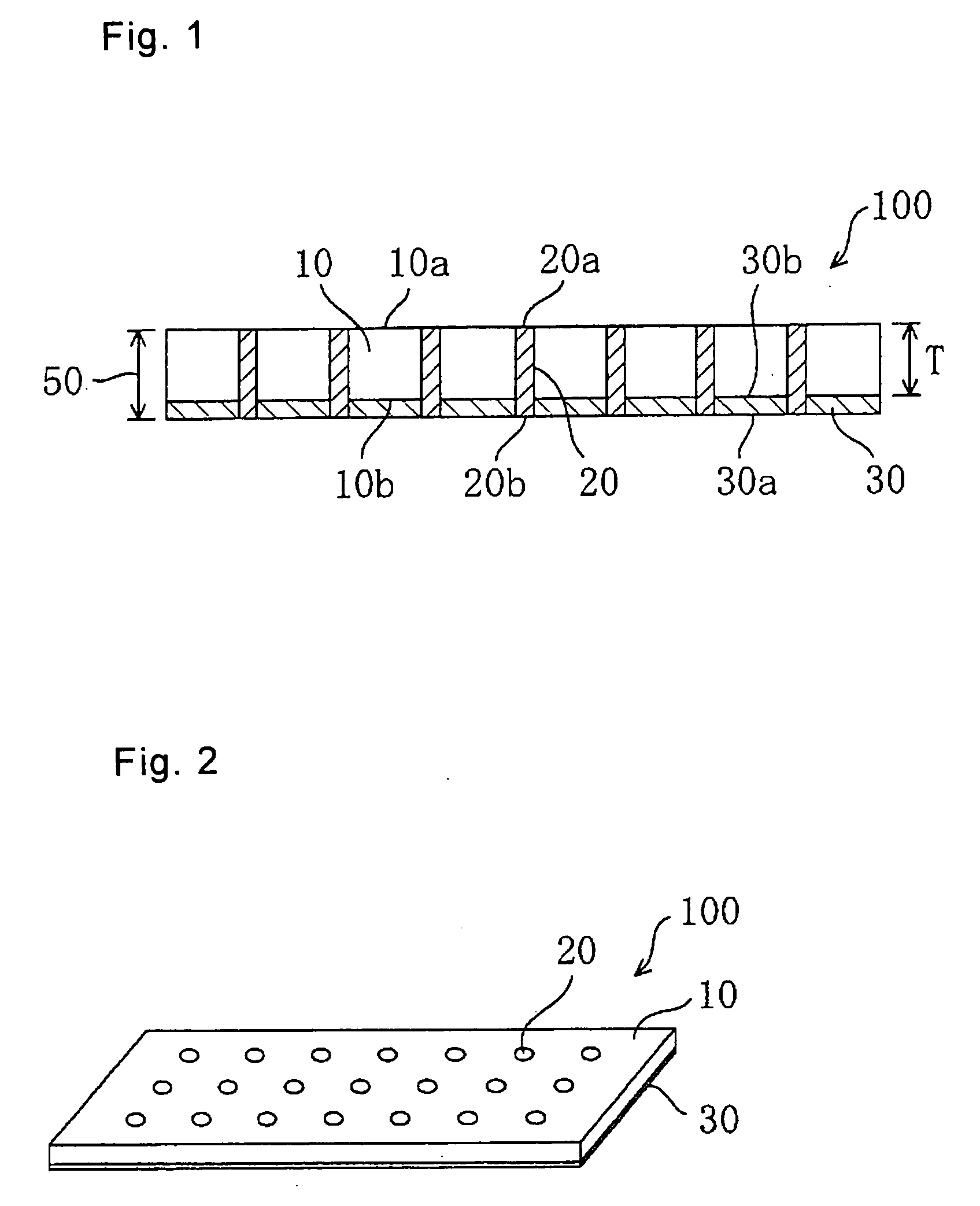
The connector sheet of Embodiment 1 according to the present invention is explained with reference to FIGS. 1 and 2. FIG. 1 schematically shows a cross-sectional view of the connector sheet 100 of this embodiment, and FIG. 2 schematically shows a perspective view of such connector sheet 100.

The connector sheet 100 of the shown embodiment includes a sheet substrate 10 and a plurality of conductive members 20. Each of the front surface 10a and the rear surface 10b of the sheet substrate 10 has the tackiness under the first condition. Under “the first condition”, the curing reaction of the thermoset resin of the front surface 10a and the rear surface 10b is not completed (and therefore the curing reaction may proceed, but does not reach the so-called C-stage state), so that the adhesiveness as described above and below is not developed. Preferably, under the first condition, no curing reaction occurs (or proceeds). As a result, the first condition ensures the tackiness of the surfac...

embodiment 2

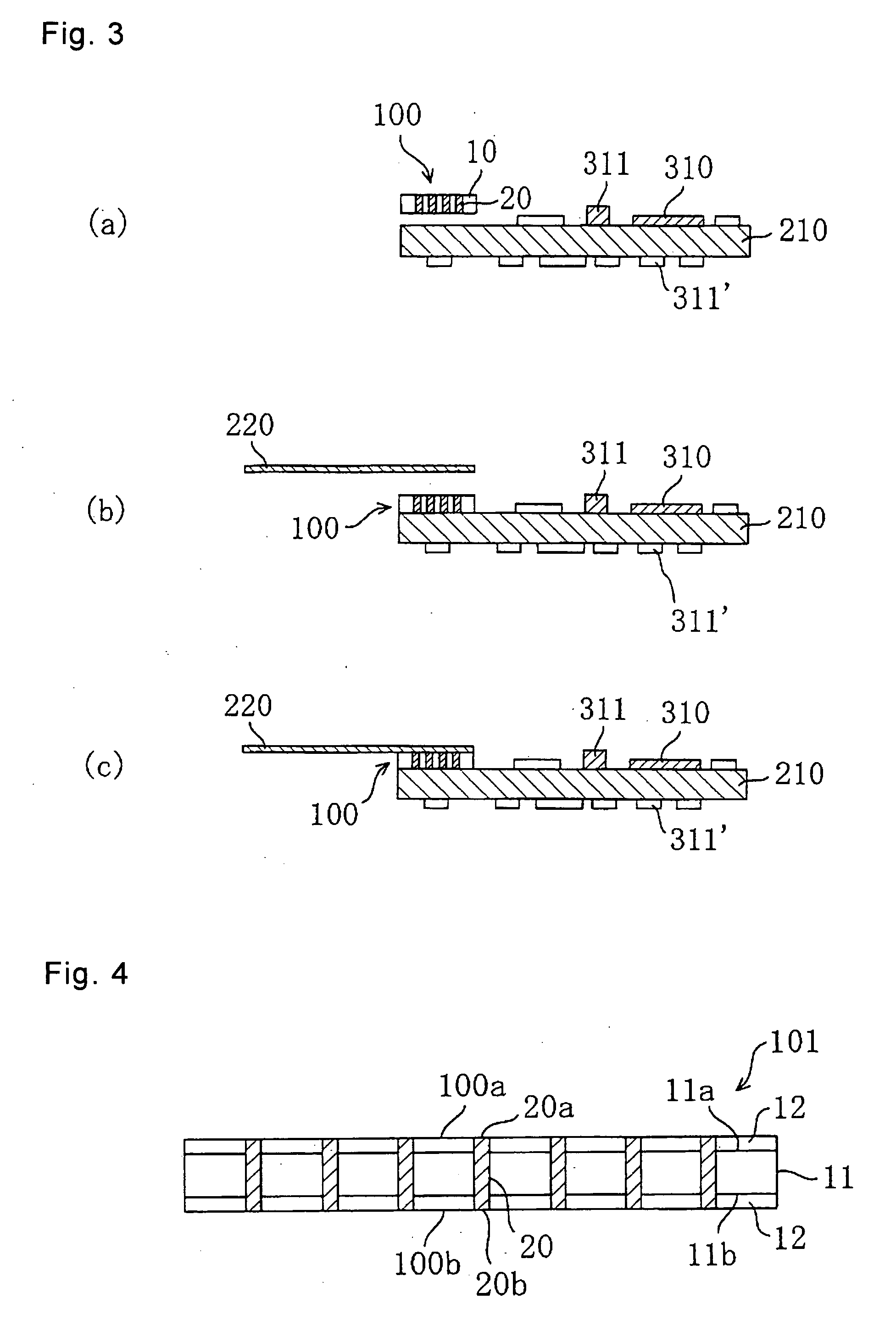
Although Embodiment 1 has explained the connector sheet 100 of which sheet substrate 10 is entirely made of the same material, the connector sheet according to the present invention basically functions as far as the front surface and the rear surface of the sheet substrate of the connector sheet have the tackiness under the first condition and also develop the adhesiveness under the second condition as described above. Thus, the connector sheet is not limited to the embodiment shown in FIG. 1, and it may have a configuration as shown in FIGS. 4 to 6.

As shown in FIGS. 4 to 6 for example, the sheet substrate of the connector sheet according to the present invention may be composed of plural kinds of materials and / or plural layers in place of a single sheet substrate 10 as shown in FIG. 1.

The connector sheet 101 shown in FIG. 4 comprises a sheet member 11 as a middle layer, and a tacky layer 12 placed on each of the front surface 11a and the rear surface 11b of the sheet member 11...

embodiment 3

With reference to FIGS. 7 and 8, a process of connecting a wiring board while using the connector sheet according to the present invention will be described.

FIGS. 7(a) to 7(c) are schematic cross-sectional views which show the steps of the process wherein the connector sheet according to the present invention and a spacer substrate are used so as to electrically connect wiring board elements, whereby a product multi-layered wiring boar (or module) is produced.

First, the connector sheets 100 of Embodiment 1 and the spacer substrate 400 are prepared. The connector sheet 100 may be replaced with the connector sheet 101, 102 or 103 of Embodiment 2. The spacer substrate 400 functions to connect wiring boards (such as printed circuit boards) while keeping some spacing between the boards, and the shown spacer substrate 400 includes no electronic part. The shown spacer substrate 400 comprises a conductor such as a via hole conductor or wiring 420 which is located in the through hole pa...


PUM

PropertyMeasurementUnit
temperatureaaaaaaaaaa

Abstract

There is provided a connector sheet which includes an insulation sheet substrate having a front surface and a rear surface opposing to the front surface, and electrically conductive members each passing through the sheet substrate along a thickness direction of the sheet substrate, and the front surface and the rear surface contain a thermoset resin, and have tackiness under a first condition and develop adhesiveness under a second condition which is different from the first condition.

Description

CROSS-REFERENCE TO RELATED APPLICATIONS The present application claims priorities under 35 U.S.C. § 119 based on: (1) Japanese Patent Application No. 2003-321326 (fined on Sep. 12, 2003, entitled “CONNECTOR SHEET, MODULE COMPRISING SUCH CONNECTOR SHEET, METHOD OF ELECTRICALLY CONNECTING CIRCUIT BOARD AND PROCESS OF PRODUCING MODULE COMPRISING CIRCUIT BOARD”, and (2) Japanese Patent Application No. 2004-015265 (fined on Jan. 23, 2004, entitled “MULTI-LAYERED WIRING BOARD, MODULE COMPRISING MULTI-LAYERED WIRING BOARD AND PROCESS OF PRODUCING MODULE”. The contents of those applications are incorporated herein by references in their entirety. BACKGROUND OF THE INVENTION 1. Field of the Invention The present invention relates to a connector sheet as a connection element and also a production process of such connector sheet which electrically connects an electric member to other electric member. Generally, such electric element is located on a wiring board, and a portion of the elect...

Claims


Application Information

Patent Timeline
Patent Type & Authority Applications(United States)
IPC IPC(8): H05K1/02H05K3/20H05K3/32H05K3/36H05K3/46
CPCH01L2924/19105Y10T29/49126H05K3/20H05K3/321H05K3/361H05K3/368H05K3/4614H05K3/4617H05K3/4652H05K3/4694H05K2201/09945H05K2201/09972H05K2201/10378H01R12/523H05K1/0268H01L2224/16227H01L2224/73204H01L2924/15313
Inventor NAKATANI, SEIICHINISHIYAMA, TOUSAKU
Owner PANASONIC CORP
Why Eureka
Try Eureka