
Low power programming technique for a floating body memory transistor, memory cell, and memory array

a programming technique and floating body technology, applied in semiconductor devices, digital storage, instruments, etc., can solve the problems of low power consumption of memory cells when programming logic, and relatively large consumption

Active Publication Date: 2005-03-24
MICRON TECH INC
View PDF99 Cites 218 Cited by
  • Summary
  • Abstract
  • Description
  • Claims
  • Application Information

AI Technical Summary

Benefits of technology

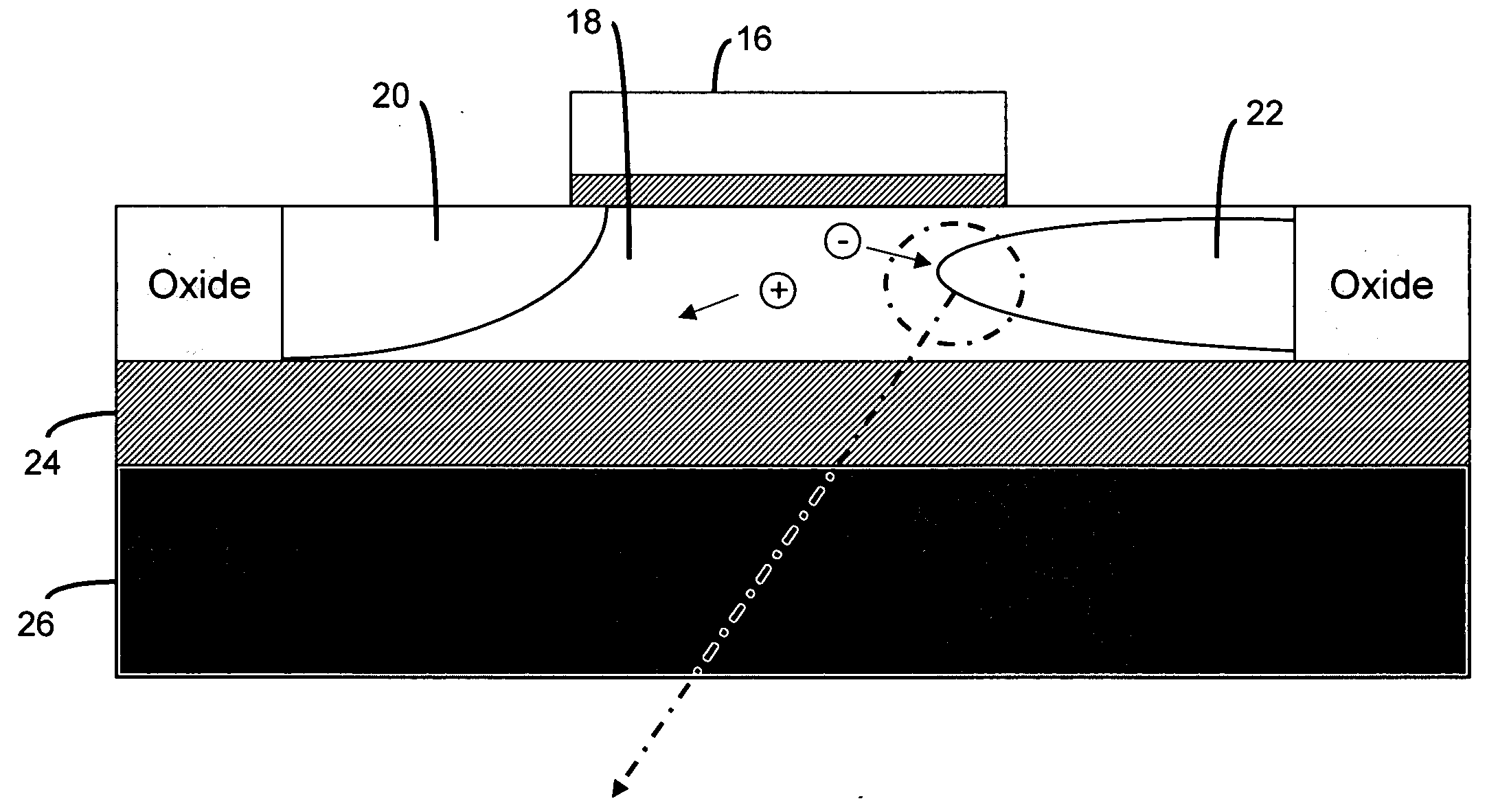
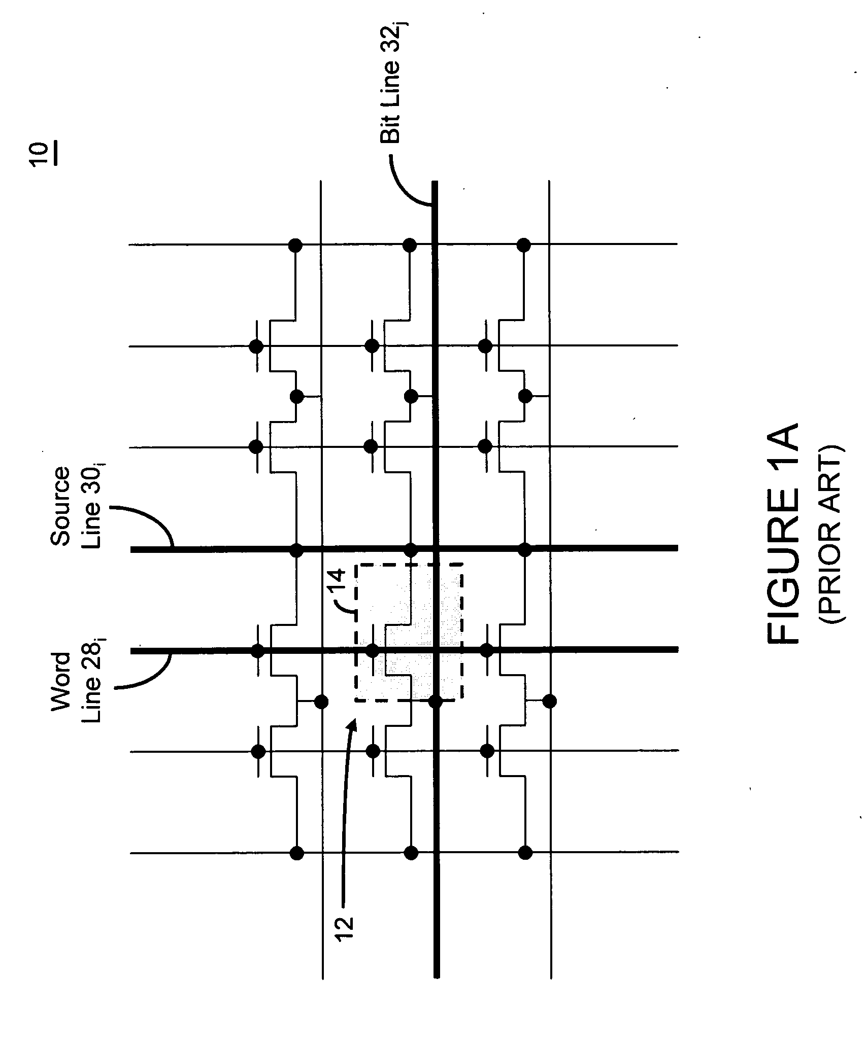
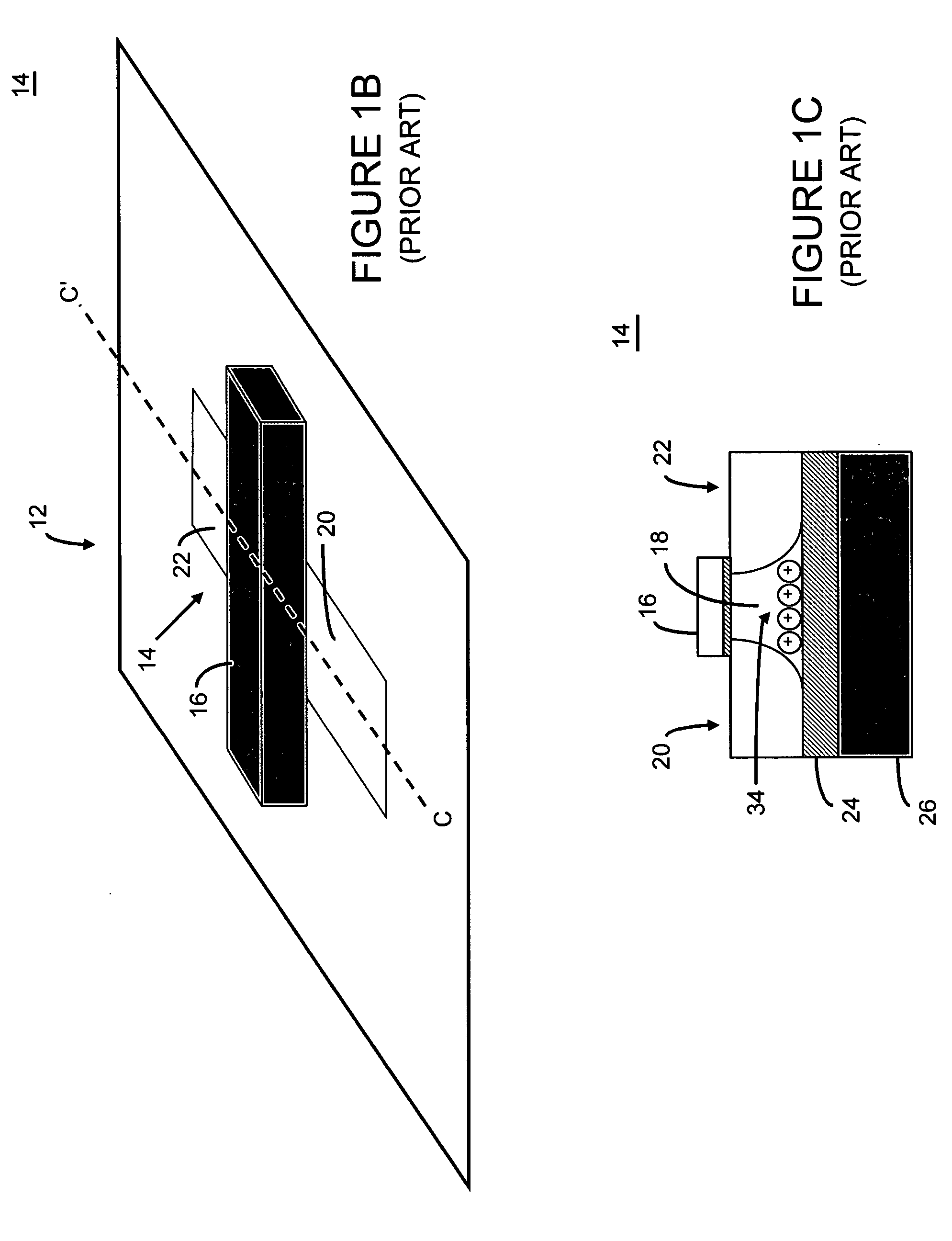
The present invention is a dynamic random access memory cell that stores two data states using an electrically floating body transistor. The transistor has a source region, a drain region, a body region disposed between the source and drain regions, and a gate capacitively coupled to the body region. The transistor has two data states that represent different amounts of majority carriers in the body region. The first data state is achieved by applying a first voltage to the gate, a second voltage to the drain region, and a third voltage to the source region. The second data state is achieved by impact ionization or band-to-band tunneling of majority carriers from the source region to the body region. The difference between the first and second data states is substantially less than the threshold voltage of the transistor. The transistor may be an N-channel or P-channel type transistor. The method of controlling the transistor includes applying the first, second, and third voltages to the gate, drain region, and source region.

Problems solved by technology

While electrically floating body transistors of memory cells (for example, SOI transistors) of the type described above have low leakage current characteristics, such memory cells consume power when programming a logic low (i.e., removing charge carriers from the body of the SOI device).
Moreover, given the need for a sufficiently large programming window (i.e., the difference in current level between a logic high and logic low), that consumption may be relatively large.

Method used


Image

  • Low power programming technique for a floating body memory transistor, memory cell, and memory array
  • Low power programming technique for a floating body memory transistor, memory cell, and memory array
  • Low power programming technique for a floating body memory transistor, memory cell, and memory array

Examples


Embodiment Construction

[0043] At the outset, it should be noted that there are many inventions described herein as well as many aspects and embodiments of those inventions. In a first aspect, the present invention is directed to a memory cell, architecture, and / or array and / or technique of writing or programming data into the memory cell (for example, a technique to write or program a logic low or State “0” in a memory cell employing an electrically floating body transistor. In this regard, the present invention programs a logic low or State “0” in the memory cell while the electrically floating body transistor is in the “OFF” state or substantially “OFF” state (for example, when the device has no (or practically no) channel and / or channel current between the source and drain). In this way, the memory cell may be programmed whereby there is little to no current / power consumption by the electrically floating body transistor and / or from memory array having a plurality of electrically floating body transisto...


PUM


Abstract

There are many inventions described and illustrated herein. In one aspect, the present invention is directed to a memory cell, architecture, and / or array and / or technique of writing or programming data into the memory cell (for example, a technique to write or program a logic low or State “0” in a memory cell employing an electrically floating body transistor. In this regard, the present invention programs a logic low or State “0” in the memory cell while the electrically floating body transistor is in the “OFF” state or substantially “OFF” state (for example, when the device has no (or practically no) channel and / or channel current between the source and drain). In this way, the memory cell may be programmed whereby there is little to no current / power consumption by the electrically floating body transistor and / or from memory array having a plurality of electrically floating body transistors.

Description

CROSS-REFERENCE TO RELATED APPLICATIONS [0001] This application claims priority to: U.S. Provisional Application Ser. No. 60 / 505,679, entitled “Low Power Programming Technique for a One Transistor SOI Memory Device”, filed Sep. 24, 2003 (hereinafter “the Provisional Application”). The contents of the Provisional Application are incorporated by reference herein in their entirety.BACKGROUND [0002] This invention relates to a semiconductor memory cell, array, architecture and device, and techniques for controlling and / or operating such cell and device; and more particularly, in one aspect, to a semiconductor dynamic random access memory (“DRAM”) cell, array, architecture and / or device wherein the memory cell includes an electrically floating body in which an electrical charge is stored. [0003] There is a continuing trend to employ and / or fabricate advanced integrated circuits using techniques, materials and devices that improve performance, reduce leakage current and enhance overall sc...

Claims


Application Information

Patent Timeline
Patent Type & Authority Applications(United States)
IPC IPC(8): G11C11/404H10B12/00
CPCG11C11/404G11C2211/4016H01L29/7841H01L27/10802H01L27/108H10B12/20H10B12/00
Inventor FAZAN, PIERREOKHONIN, SERGUEI
Owner MICRON TECH INC
Learn More