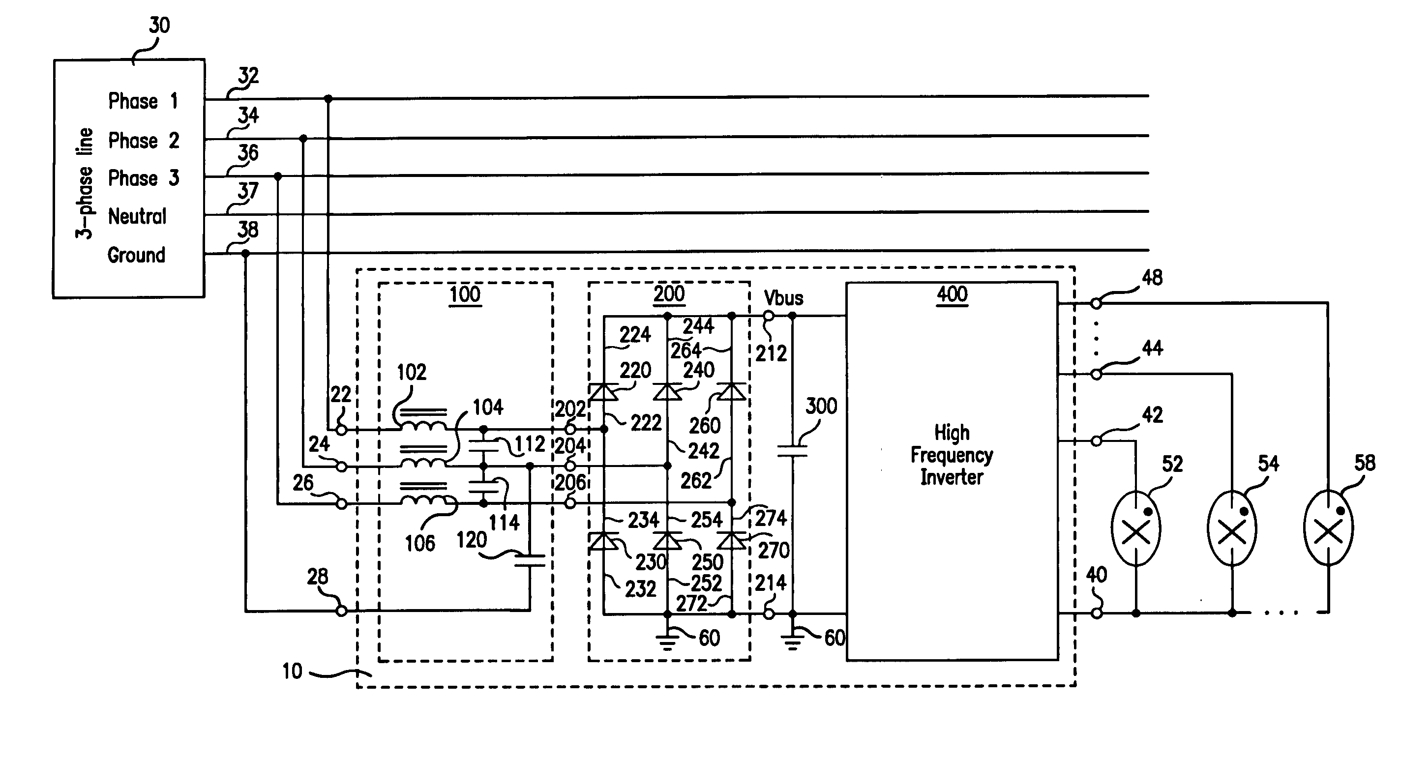
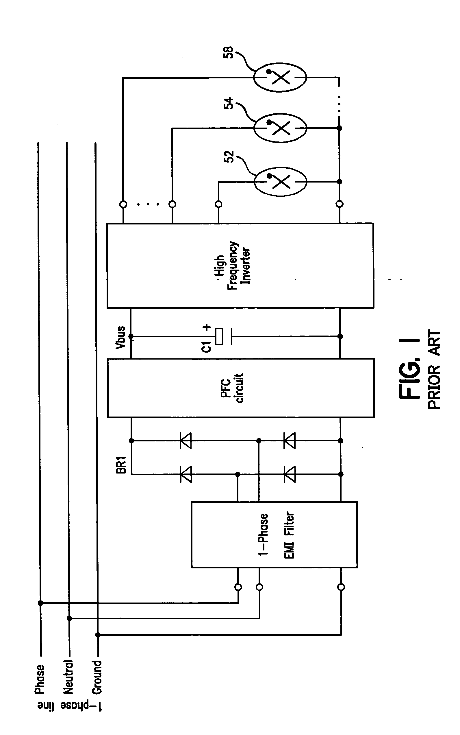
[0014] A ballast 10 for powering at least one gas discharge lamp 52 from a three-phase alternating current (AC) voltage source 30 is described in FIG. 4. Ballast 10 comprises a three-phase rectifier circuit 200, a high frequency filter capacitor 300, and a high frequency inverter 400. Three-phase AC voltage source 30 is a conventional 60 hertz voltage source that is provided by the electrical utility company.
[0015] In a preferred embodiment of ballast 10, three-phase rectifier circuit 200 comprises a first input terminal 202, a second input terminal 204, a third input terminal 206, a first output terminal 212, a second output terminal 214, a first diode 220, a second diode 230, a third diode 240, a fourth diode 250, a fifth diode 260, and a sixth diode 270. First input terminal 202 is adapted to receive a first phase 32 of three-phase AC voltage source 30. Second input terminal 204 is adapted to receive a second phase 34 of source 30. Third input terminal is adapted to receive a third phase 36 of AC source 30. First diode 220 has an anode 222 coupled to first input terminal 202 and a cathode 224 coupled to first output terminal 212. Second diode 230 has an anode 232 coupled to second output terminal 214 and a cathode 243 coupled to first input terminal 202. Third diode 240 has an anode 242 coupled to second input terminal 204 and a cathode 244 coupled to first output terminal 212. Fourth diode 250 has an anode 252 coupled to second output terminal 214 and a cathode 254 coupled to second input terminal 204. Fifth diode 260 has an anode 262 coupled to third input terminal 206 and a cathode 264 coupled to first output terminal 212. Sixth diode 270 has an anode 272 coupled to second output terminal 214 and a cathode 274 coupled to third input terminal 206.
[0016] During operation, rectifier circuit 200 receives the three-phase alternating current (AC) voltage source 30 and provides a rectified output voltage. As described in FIG. 5, the rectified output voltage, Vbus, has a maximum value, a minimum value, an average value (Vavg), and a ripple value (ΔV). In ballast 10, the ripple value (ΔV), which is defined as the difference between the maximum value and the minimum value, has a root-mean-square (RMS) value that is no greater than about 5% of the average value Vavg. Advantageously, rectifier circuit 200 utilizes all three phases 32,34,36 of the AC source 30 to provide a Vbus that naturally has a small amount of 360 hertz ripple and that therefore requires no capacitive filtering in order to provide an acceptably low level of visible flicker in the illumination of the lamp(s). This is in contract with the prior art ballast of FIG. 1 where, in the absence of a large electrolytic capacitor C1, the 120 hertz ripple would be extremely high, with consequent excessive flicker in the illumination of the lamp(s).
[0017] Referring to FIG. 4, high frequency filter capacitor 300 is coupled between the first and second output terminals 212,214 of rectifier circuit 200. The sole function of capacitor 300 is to provide an AC path for high frequency current drawn by inverter 400. Capacitor 300 can thus be realized by a capacitor with a relatively low capacitance value (e.g., 0.1 microfarads when ballast 10 is designed to power four 32 watt lamps). Consequently, capacitor 300 can be implemented by a film capacitor or a ceramic capacitor. Advantageously, because ballast 10 does not require an electrolytic bulk capacitor, its operating life will be substantially greater than the prior art ballast described in FIG. 1, if the ballast is operated in a high ambient temperature environment. Moreover, because of the relatively low capacitance of capacitor 300, the amount of inrush current that occurs in ballast 10 will be dramatically less than what occurs in the prior art ballast described in FIG. 1.
[0018] High frequency inverter 400 is coupled to rectifier circuit 200 and high frequency filter capacitor 300. During operation, inverter 400 powers at least one gas discharge lamp 52 and has an operating frequency that is greater than about 20,000 hertz. In general, inverter 400 includes a plurality of output terminals 40,42,44, . . . , 48 for connection to a plurality of discharge lamps 52,54, . . . , 58. Inverter 400 may be realized by any of a number of circuit arrangements (e.g., a half-bridge inverter followed by a series resonant output circuit) that are well known to those skilled in the art of electronic ballasts.
[0019] During operation of ballast 10, the line current that is drawn from each phase 32,34,36 of AC source 30 has a total harmonic distortion (THD) that is no greater than about 33%. Additionally, as the line current drawn from each phase is only moderately out of phase with the voltage between each phase and ground 38, ballast 10 provides a power factor (PF) that is no less than about 0.9. Thus, ballast 10 is capable of approaching or meeting applicable standards for power quality without requiring an active power factor correction (PFC) circuit such as a boost converter. Consequently, in comparison with the prior art electronic ballast described in FIG. 1, ballast 10 provides the added benefits of lower material cost, smaller physical size, and enhanced energy efficiency (e.g., 94% versus about 88% for the ballast of FIG. 1).
[0020] Preferably, as described in FIG. 4, ballast 10 further comprises a three-phase electromagnetic interference (EMI) filter 100 that is interposed between rectifier circuit 200 and three-phase AC voltage source 30. During operation, three-phase EMI filter 100 attenuates any line-conducted EMI that tends to arise due to the high frequency operation of inverter 400. In a preferred embodiment of ballast 10, three-phase EMI filter comprises first, second, third, and fourth input connections 22,24,26,28, first, second, and third inductors 102,104,106, and first, second, and third capacitors 112,114,120. First input connection 22 is adapted to receive a first phase 32 of three-phase AC voltage source 30. Second input connection is adapted to receive a second phase of source 30. Third input connection is adapted to receive a third phase of source 30. Fourth input connection is adapted to receive a ground 38 of source 30. A neutral 37 of source 30 has no corresponding connection to ballast 10. First inductor 102 is coupled between first input connection 22 and the first input terminal 202 of rectifier circuit 200. Second inductor 104 is coupled between second input connection 24 and the second input terminal 204 of rectifier circuit 200. Third inductor 106 is coupled between third input connection 26 and the third input terminal 206 of rectifier circuit 200. First capacitor 112 is coupled between the first and second input terminals 202,204 of rectifier circuit 200. Second capacitor 114 is coupled between the second and third input terminals 204,206 of rectifier circuit 200. Third capacitor 120 is coupled between fourth input connection 28 and the second input terminal 204 of rectifier circuit 200.
[0021] Turning now to FIG. 6, it can be seen that ballast 10 allows for installations in which all of the fixtures in a building are wired to the AC source 30 in an identical manner. This is in contrast to the arrangement described in FIG. 3, where the fixtures must be segregated into three groups in order to equalize the loading on each phase of the AC source. Thus, ballast 10 provides the added benefit of simplifying the electrical wiring that is routed to the lighting fixtures within a building.
[0022] Although the present invention has been described with reference to certain preferred embodiments, numerous modifications and variations can be made by those skilled in the art without departing from the novel spirit and scope of this invention.