Echo clock on memory system having wait information

Inactive Publication Date: 2005-03-31
POLARIS INNOVATIONS LTD
View PDF6 Cites 47 Cited by
  • Summary
  • Abstract
  • Description
  • Claims
  • Application Information

AI Technical Summary

Problems solved by technology

However, an addition of the DQS signal increases the pin count of the memory and system controller and a width of the system bus, as well as may compromise timing relationship between the data strobe signal and the data.

Method used


Image

  • Echo clock on memory system having wait information
  • Echo clock on memory system having wait information
  • Echo clock on memory system having wait information

Examples


Embodiment Construction

[0028] The present invention generally provides methods and circuit configurations for implementing a double data rate feature in memory devices capable of operating in a variable latency mode in Read and / or Write cycles, such as burst PSRAM devices.

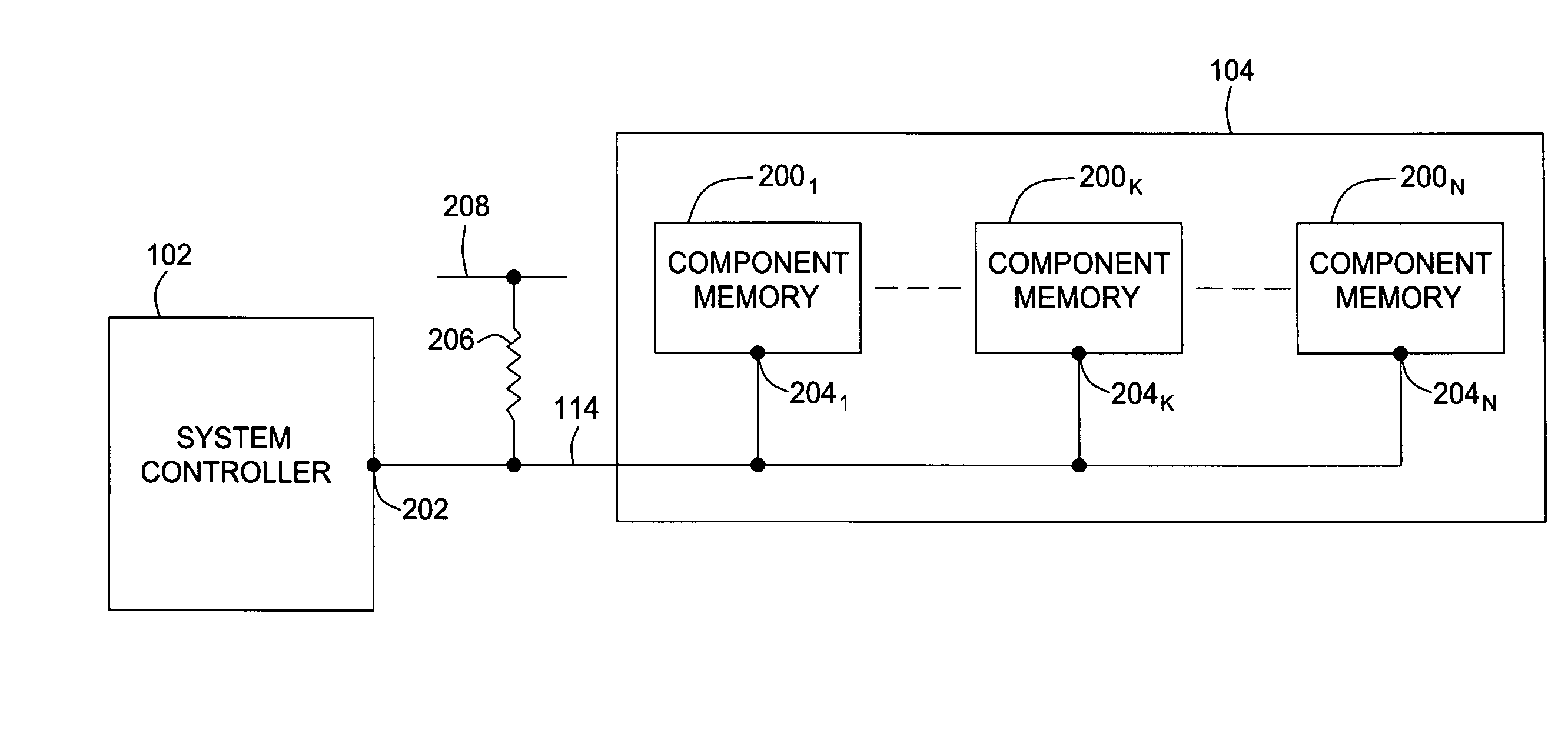
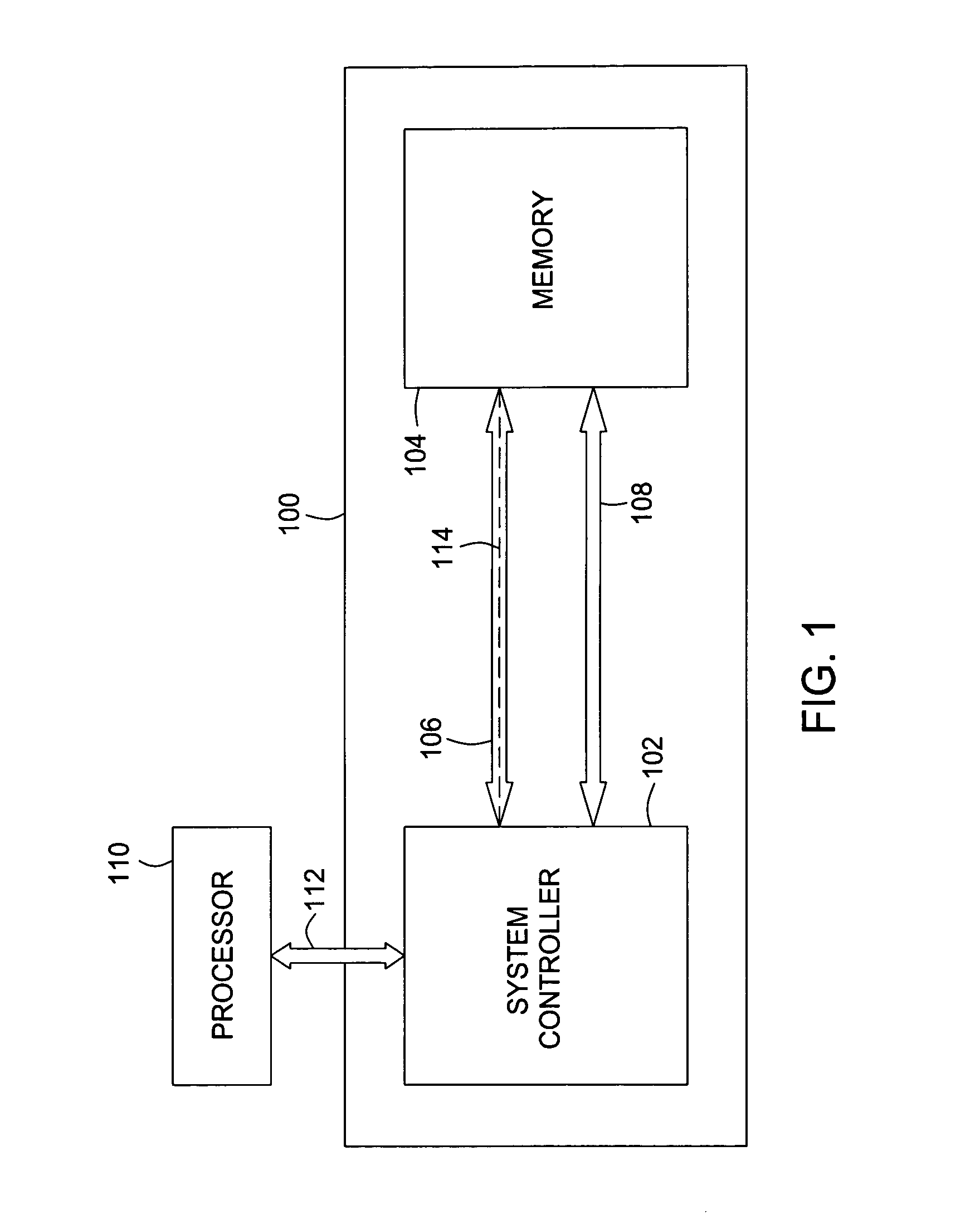
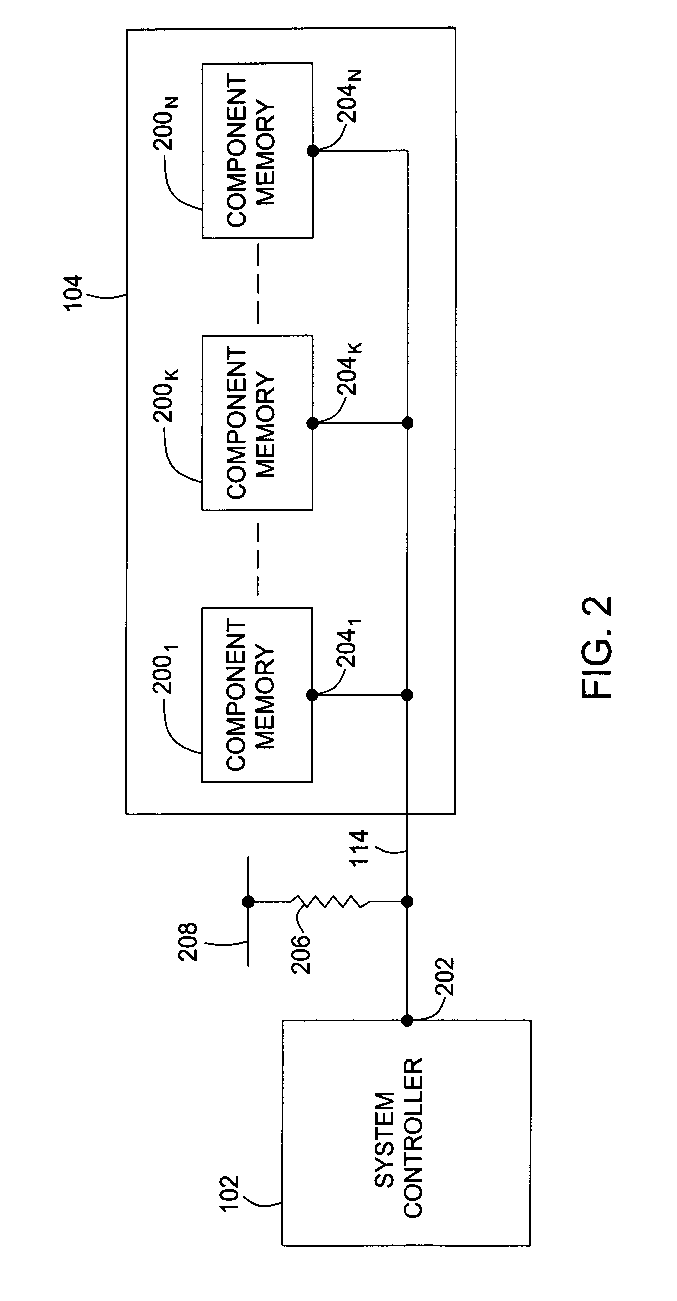
[0029]FIG. 1 depicts a simplified functional block diagram of a system 100 using a burst PSRAM device 104. In one embodiment, the system 100 generally comprises a system controller 102, a memory 104, an address / command (i.e., system) bus 106, and a data (i.e., DQ) bus 108. The memory 104 may comprise one or more component memories (discussed below in reference to FIG. 2), where each component memory is coupled to the buses 106 and 108. The system bus 106 may comprise unidirectional and bi-directional transmission lines, while the DQ bus includes bi-directional transmission lines. The system controller 102 is typically coupled to a processor of an external electronic device 110 (e.g., computer, cell phone, and the like) using an applicat...


PUM


Abstract

A method and a circuit configuration for implementing a double data rate feature in a memory device capable of operating in a variable latency mode. The memory device may utilize a WAIT_DQS signal that combines functionality of a WAIT signal indicating when valid data is present on a data bus in Read cycle and the memory is ready to accept data in Write cycle, and a data strobe (DQS) signal.

Description

BACKGROUND OF THE INVENTION [0001] 1. Field of the Invention [0002] The present invention generally relates to integrated circuit memory devices and, more particularly, to Pseudo Static random access memory (PSRAM) devices operating in a burst access mode (“burst PSRAM”). [0003] 2. Description of the Related Art [0004] In portable applications, such as handheld / wireless devices, the use of low power consuming memory is essential. A PSRAM device meets both low power consumption and high density requirements. A PSRAM, like a conventional dynamic random access memory (DRAM), contains dynamic memory cells but, in terms of interface and packaging, has the appearance of a static random access memory (SRAM). In the PSRAM, a refresh operation that is commonly required to maintain the stored information in dynamic memory cells is facilitated using internal means and, as such, is transparent to a system controller of the memory. Further, a PSRAM may operate in a burst mode. The burst mode enh...

Claims


Application Information

Patent Timeline
Patent Type & Authority Applications(United States)
IPC IPC(8): G06F13/16G06F13/42G11C7/00G11C7/10G11C8/00
CPCG11C7/1051G11C7/1063G11C7/1066G11C7/1093G11C7/1078G11C7/109G11C7/1072
Inventor OH, JONG-HOON
Owner POLARIS INNOVATIONS LTD
Why Eureka
Try Eureka