Easily loaded and unloaded getter device for reducing evacuation time and contamination in a vacuum chamber and method for use of same
a vacuum chamber and getter technology, applied in the direction of ion implantation coating, chemical vapor deposition coating, coating, etc., can solve the problems of reducing the quantity requiring substantial modifications, and reducing the amount of residual adsorbed gas on the surface of the chamber, etc., to achieve easy loading and unloading, reduce evacuation time and contamination, and high surface area
- Summary
- Abstract
- Description
- Claims
- Application Information
AI Technical Summary
Benefits of technology
Problems solved by technology
Method used
Image
Examples
example 1
The pressure in a PVD deposition chamber was continuously monitored while a pump-down cycle was performed. The measured pressure in the chamber during this cycle is shown in FIG. 9 as curve 1. The chamber included a pedestal supporting a sample-holder and further included an internal electrical resistance heater. The chamber also included two quartz lamps located on two opposing side walls. A rotary pump and a cryogenic pump were connected to the chamber by a port to perform the pump-down. In order to measure pressures in the chamber below about 10−5 mbar a Bayard-Alpert manometer was employed.
At the beginning of the test the chamber was sealed and pumping was initiated. Approximately a half hour into the test, when the pressure in the chamber reached a value of about 10−6 mbar, a baking procedure was performed by heating the interior of the chamber with the quartz lamps and heating the electrical resistance heater to 500° C. After a two hour bake the chamber was allowed to cool ...
example 2
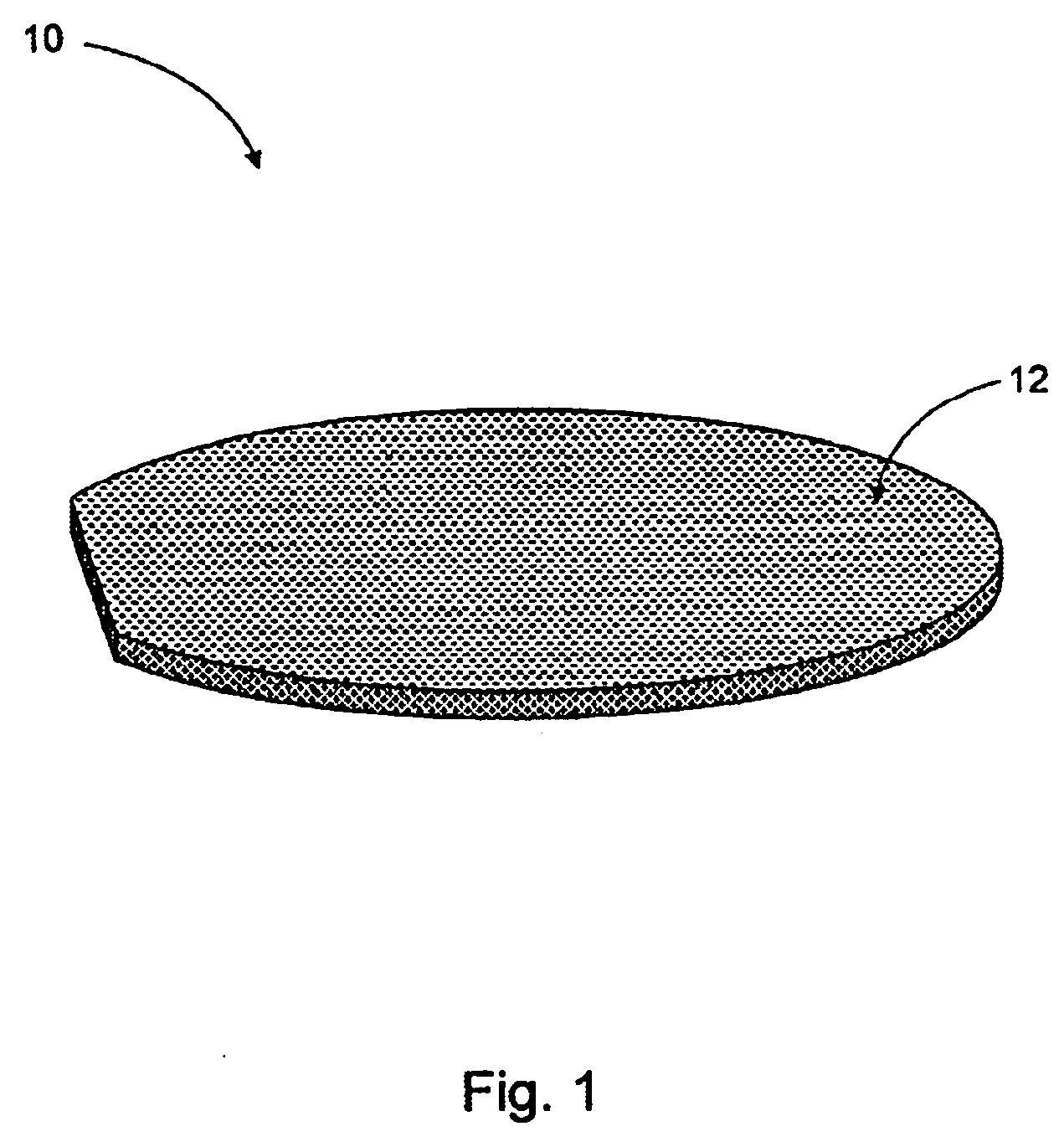
The pressure in the PVD deposition chamber used in Example 1 was continuously monitored while a pump-down cycle using a getter device of the present invention was performed. The measured pressure in the chamber during this cycle is shown in FIG. 9 as curve 2. Initially, a non-activated getter device was placed on the sample holder within the chamber. The getter device consisted of a silicon wafer support having a diameter of about 200 mm and a deposit of getter material on one face. The getter material used was St 121, described above, and was deposited by screen printing to create a layer approximately 150 μm thick. The evacuation procedure described in Example 1 was then repeated. During the baking procedure, the temperature of the getter device was raised to about 500° C., primarily by the internal electrical resistance heater. The getter material was thus activated during the baking.
From Curve 2 in FIG. 9 it can be seen that during the bake the pressure in the chamber increas...
PUM
| Property | Measurement | Unit |
|---|---|---|
| thickness | aaaaa | aaaaa |
| thickness | aaaaa | aaaaa |
| thickness | aaaaa | aaaaa |
Abstract
Description
Claims
Application Information


