

Electron emitter
a technology of electron emitter and emitter, which is applied in the manufacture of electric discharge tubes/lamps, instruments, and tubes with screens, etc., can solve the problems of low energy required for electron emitting, complex panel fabrication process, and high panel fabrication cost, and achieves easy production of high electric field concentration, large output, and high efficiency
- Summary
- Abstract
- Description
- Claims
- Application Information
AI Technical Summary
Benefits of technology
Problems solved by technology
Method used
Image

Examples
first embodiment
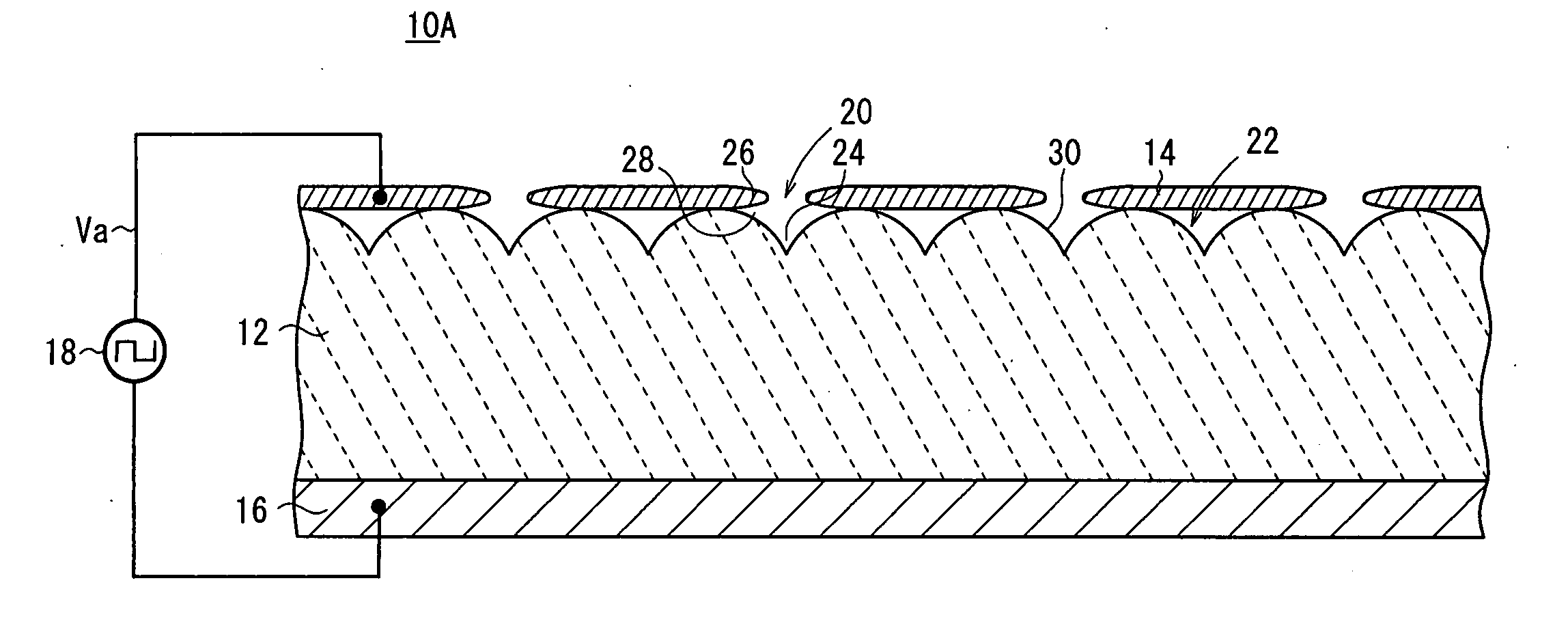
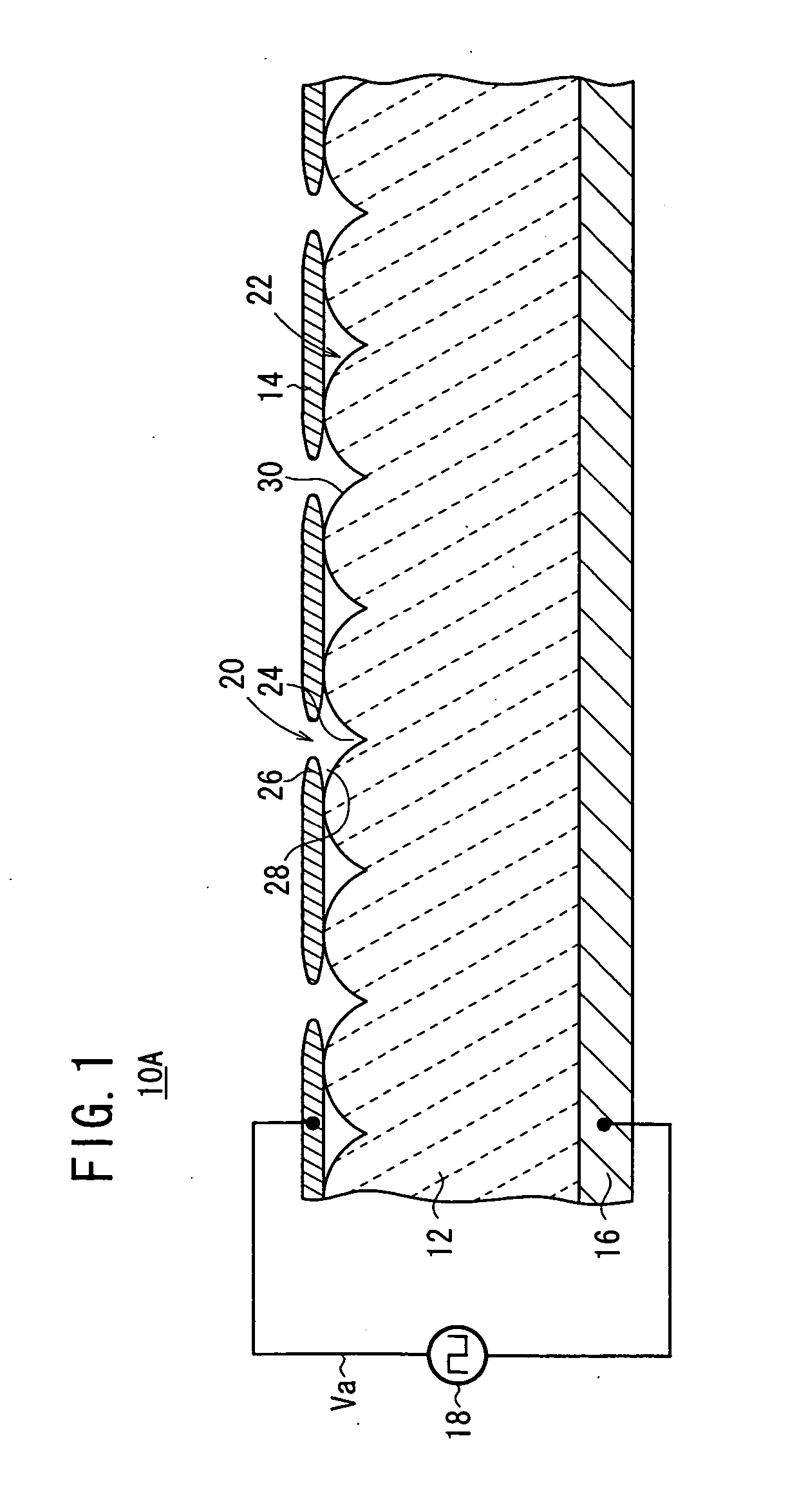
As shown in FIG. 1, an electron emitter 10A comprises a plate-like emitter (a substance serving as an emitter) 12 made of a dielectric material, a first electrode (e.g., an upper electrode) 14 formed on a first surface (e.g., an upper surface) of the emitter 12, a second electrode (e.g., a lower electrode) 16 formed on a second surface (e.g., a lower surface) of the emitter 12, and a pulse generation source 18 for applying a drive voltage Va between the upper electrode 14 and the lower electrode 16.
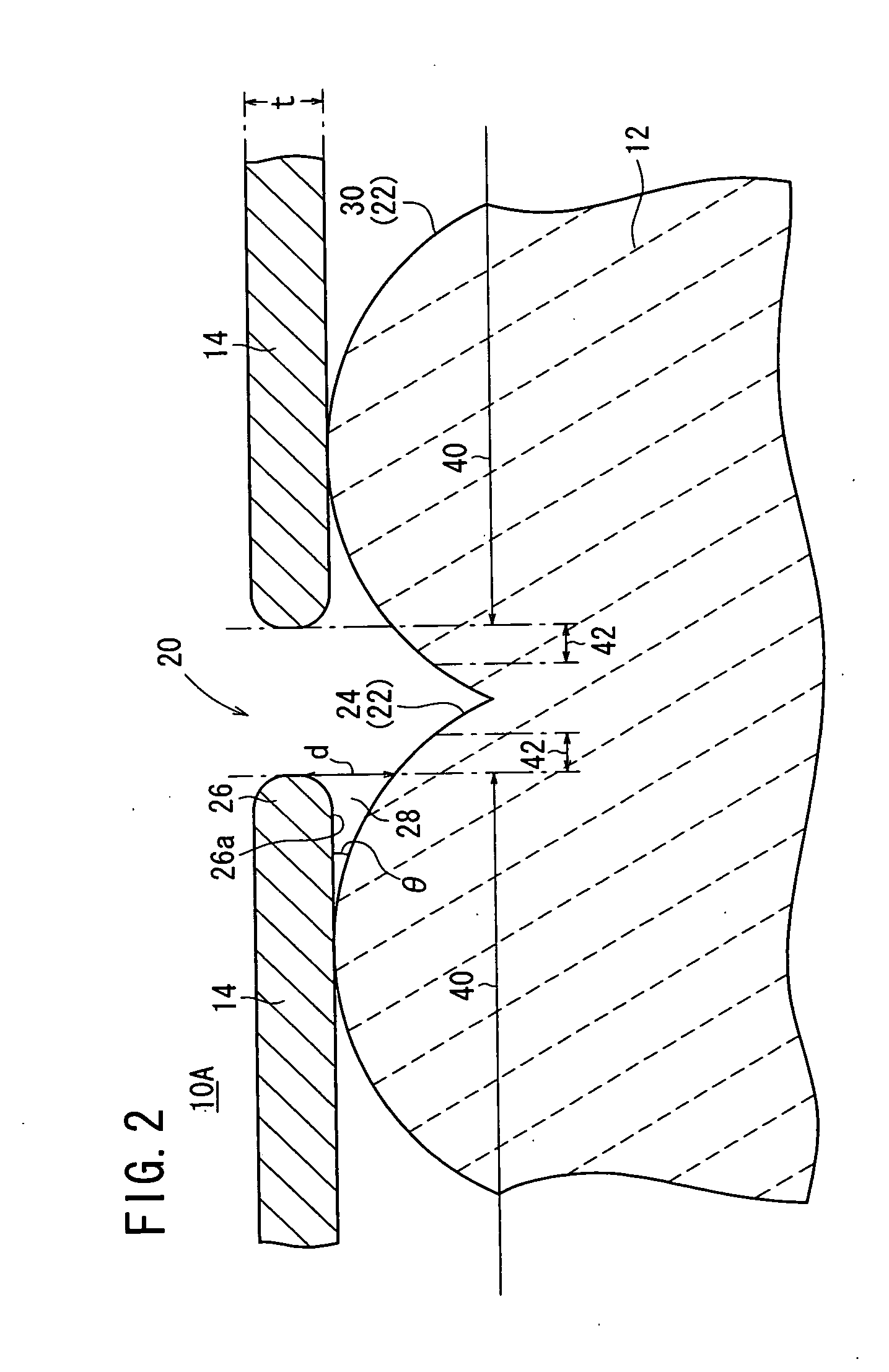
The upper electrode 14 has a plurality of through regions 20 where the emitter 12 is exposed. The emitter 12 has surface irregularities 22 due to the grain boundary of the dielectric material. The through regions 20 of the upper electrode 14 are formed in areas corresponding to concavities 24 due to the grain boundary of the dielectric material. In the embodiment shown in FIG. 1, one through region 20 is formed in association with one recess 24. However, one through region 20 may be for...
experimental examples (first through fourth experimental examples)
Four experimental examples (first through fourth experimental examples) of the electron emitter 10A according to the first embodiment will be shown.
According to the first experimental example, the emission of electrons from the electron emitter 10A was observed. Specifically, as shown in FIG. 26A, a write pulse Pw having a voltage of −70 V was applied to the electron emitter 10A to cause the electron emitter 10A to accumulate electrons, and thereafter a turn-on pulse Ph having a voltage of 280 V was applied to cause the electron emitter 10A to emit electrons. The emission of electrons was measured by detecting the light emission from the phosphor 134 with a light-detecting device (photodiode). The detected waveform is shown in FIG. 26B. The write pulse Pw and the turn-on pulse Ph had a duty cycle of 50%.
It can be seen from the first experimental example that light starts to be emitted on a positive-going edge of the turn-on pulse Ph and the light emission is finished in an initia...
second embodiment
An electron emitter 10B will be described below with reference to FIG. 33.
As shown in FIG. 33, the electron emitter 10B according to the second embodiment is of an arrangement that is essentially the same as the electron emitter 10A according to the first embodiment, but is characterized in that the upper electrode 14 has a thickness t greater than 40 μm, and the through region 20 is artificially formed by etching (wet etching or dry etching), liftoff, laser, etc. The through region 20 may be shaped as the hole 32, the recess 44, or the slit 48.
The lower surface 26a of the peripheral portion 26 of the through region 2 in the upper electrode 14 is inclined progressively upwardly toward the center of the through region 20. This shape may simply be formed by liftoff, for example.
The electron emitter 10B according to the second embodiment is capable of easily producing a high electric field concentration as with the electron emitter 10A according to the first embodiment. The elect...
PUM
 Abstract
Description
Claims
Application Information