Light source

a technology for light sources and discharge tubes, applied in the field of light sources, can solve the problems of high panel fabrication costs, unstable electron emission, and inability to use electron emitters, and achieve the effect of increasing reliability and long service li

Inactive Publication Date: 2007-06-12
NGK INSULATORS LTD
View PDF22 Cites 6 Cited by
  • Summary
  • Abstract
  • Description
  • Claims
  • Application Information

AI Technical Summary

Benefits of technology

[0009]It is an object of the present invention to provide a light source which comprises electron emitters each having an emitter made of a dielectric body, the electron emitters being prevented from emitting excessive electrons to prevent electrodes or the like from being damaged by the emission of electrons, thus allowing the light source to have a long service life and increased reliability.
[0010]Another object of the present invention is to provide a light source which is capable of easily producing a high electric field concentration and providing many electron emission spots for emitting electrons with a large output and a high efficiency.

Problems solved by technology

All of these disclosed electron emitters are disadvantageous in that since no dielectric body is employed in the emitter, a forming process or a micromachining process is required between facing electrodes, a high voltage needs to be applied to emit electrons, and a panel fabrication process is complex and entails a high panel fabrication cost.
However, the conventional electron emitters are problematic in that the electron emission is not stable and can only be performed several tens of thousands times at most, and the electron emitters are not practical when used as light sources, for example.

Method used


Image

  • Light source
  • Light source
  • Light source

Examples


first embodiment

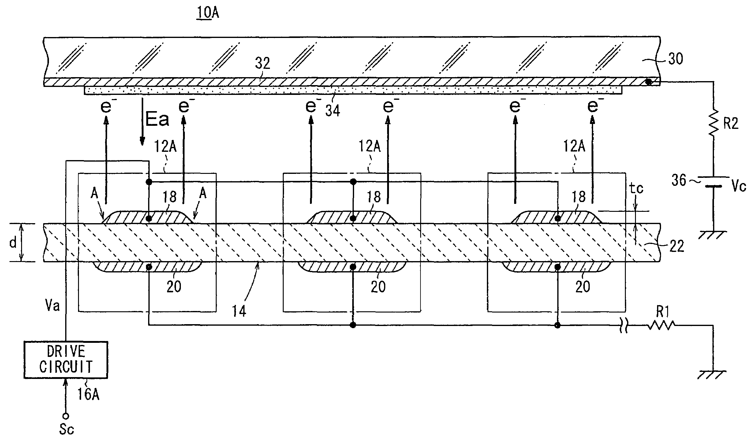
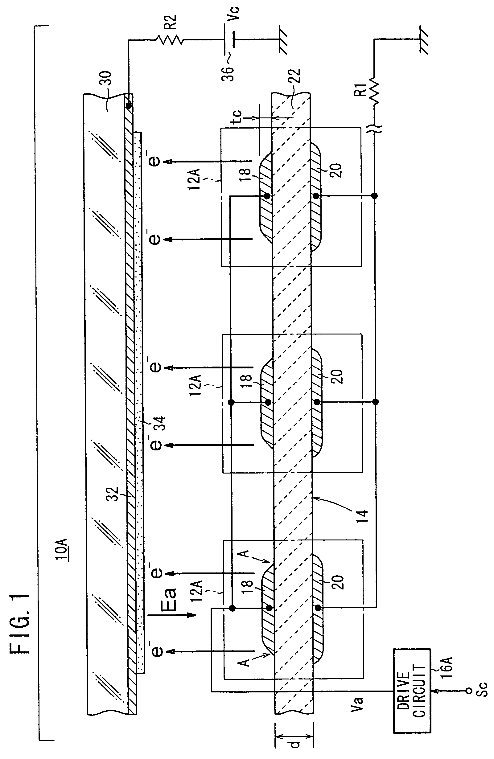
[0153]As shown in FIG. 1, a light source 10A according to the present invention has a light emitting section 14A comprising a two-dimensional array of electron emitters 12A, and a drive circuit 16A for applying a drive voltage Va to each of the electron emitters 12A of the light emitting section 14A.

[0154]The drive circuit 16A applies a drive voltage Va between a first electrode (e.g., an upper electrode) 18 and a second electrode (e.g., a lower electrode) 20 of each of the electron emitters 12A to control each of the electron emitters 12A based on a control signal Sc representative of turn-on / turn-off from an external source (a turn-on / turn-off switch or the like). Preferred examples of the drive circuit 16A will be described later on.

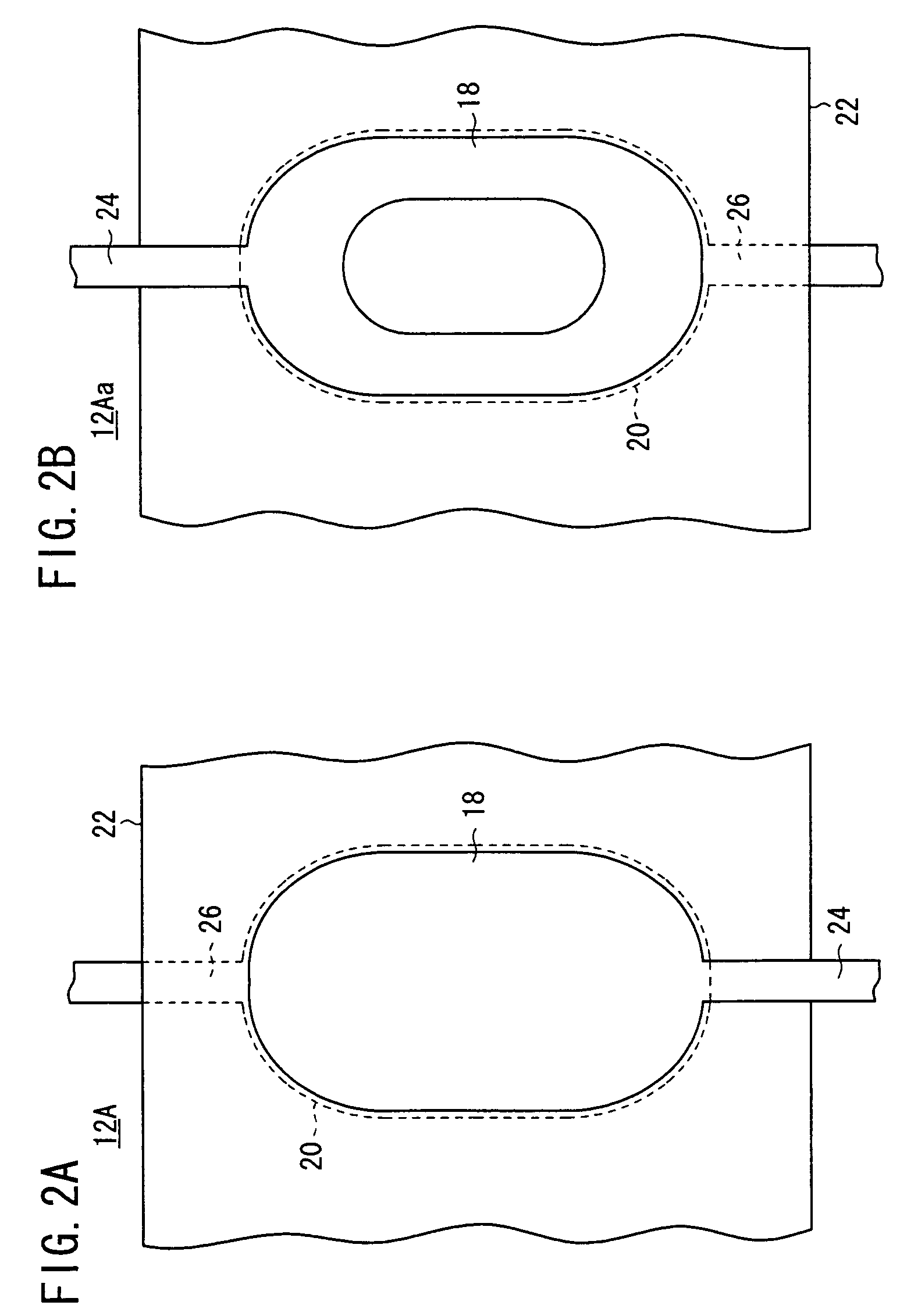
[0155]As shown in FIG. 1, each of the electron emitters 12A has a plate-like emitter 22, the upper electrode 18 disposed on a face side of the emitter 22, and the lower electrode 20 disposed on a reverse side of the emitter 22. Since the electron emit...

second embodiment

[0285]As shown in FIG. 38, each of electron emitters 12B of the light source 10B comprises an emitter 22, an upper electrode 18, a lower electrode 20, and a pulse generating source 100 for applying a drive voltage Va between the upper electrode 18 and the lower electrode 20.

[0286]The upper electrode 18 has a plurality of through regions 102 where the emitter 22 is exposed. The emitter 22 has surface irregularities 104 due to the grain boundary of a dielectric material that the emitter 22 is made of. The through regions 102 of the upper electrode 18 are formed in areas corresponding to concavities 106 due to the grain boundary of the dielectric material. In the embodiment shown in FIG. 38, one through region 102 is formed in association with one concavity 106. However, one through region 102 may be formed in association with a plurality of concavities 106. The particle diameter of the dielectric material of the emitter 22 should preferably be in the range from 0.1 μm to 10 μm, and m...

third embodiment

[0454]A preferred structure fabricated as a planar light source, i.e., a light source 10C will be described below with reference to FIGS. 78 through 81.

[0455]As shown in FIG. 78, the light source 10C according to the third embodiment has a rear glass substrate 200 and a front glass substrate 202 having a plate surface disposed in facing relation to a principal surface of the rear glass substrate 200. The plate surface of the front glass substrate 202 is coated with a white phosphor (not shown). A two-dimensional array of electron emitters 12B as shown in FIG. 38, for example, is disposed on the principal surface of the rear glass substrate 200. A vacuum is developed between the rear glass substrate 200 and the front glass substrate 202.

[0456]As shown in FIG. 79, the electron emitters 12B may comprise a two-dimensional array of rectangular electron emission units 204 (described later).

[0457]As shown in FIG. 80, each of the electron emission units 204 comprises a single ferroelectric...


PUM


Abstract

A light source has a rear glass substrate and a front glass substrate having a plate surface disposed in facing relation to a principal surface of the rear glass substrate. The plate surface of the front glass substrate is coated with a phosphor. A two-dimensional array of electron emitters is disposed on the principal surface of the rear glass substrate. A space defined between the rear glass substrate and the front glass substrate is filled with a gas. The gas may be an Hg (mercury) gas or an Xe (xenon) gas.

Description

BACKGROUND OF THE INVENTION[0001]1. Field of the Invention[0002]The present invention relates to a light source (including a planar light source) comprising electron emitters each having an upper electrode and a lower electrode that are disposed in an emitter.[0003]2. Description of the Related Art[0004]Recently, electron emitters having a drive electrode and a common electrode have been finding use in various applications such as field emission displays (FEDs) and backlight units. In an FED, a plurality of electron emitters are arranged in a two-dimensional array, and a plurality of phosphors are positioned in association with the respective electron emitters with a predetermined gap left therebetween.[0005]Conventional electron emitters are disclosed in Japanese Laid-Open Patent Publication No. 1-311533, Japanese Laid-Open Patent Publication No. 7-147131, Japanese Laid-Open Patent Publication No. 2000-285801, Japanese Patent Publication No. 46-20944, and Japanese Patent Publicatio...

Claims


Application Information

Patent Timeline
Patent Type & Authority Patents(United States)
IPC IPC(8): H01J1/02
CPCB82Y10/00H01J1/312H01J63/08H01J2201/306
Inventor TAKEUCHI, YUKIHISANANATAKI, TSUTOMUOHWADA, IWAOAKAO, TAKAYOSHI
Owner NGK INSULATORS LTD
Why Eureka
Try Eureka