Integrally packaged imaging module

a technology of imaging modules and packaging, applied in the field of imaging modules, can solve the problems of time-consuming and laborious assembly steps, and therefore cost, and conventional mechanisms for attaching imaging modules to host devices tend to be costly, and conventional imaging modules are not suitable for automatic assembly

Active Publication Date: 2005-04-14
APTINA IMAGING CORP
View PDF9 Cites 114 Cited by
  • Summary
  • Abstract
  • Description
  • Claims
  • Application Information

AI Technical Summary

Benefits of technology

[0012] Embodiments of the present invention provide an improved integrally packaged imaging module, which includes an integrated circuit (IC), including an image sensing device formed on a semiconductor substrate, and wafer level packaging enclosing the IC. The wafer level packaging includes a transparent enclosure portion adapted to permit image acquisition of an image by the image sensing

Problems solved by technology

Therefore, the assembly step is time consuming and labor-intensive, and therefore costly.
Conventional mechanisms for attaching the imaging modules to the host devices tend to be costly when compared to the costs of attaching other types of electronic/electrical hardware, such as integrated circuits (IC's).
Conventional imaging modules are not suitable for automatic assembly.
Such features are expensive, not well suited for automatic assembly, bulky, and less reliable than soldered connections.
Standard automatic electronic assembly processes are not readily adaptable to support automatic mounting and connecting of conventional imag

Method used


Image

  • Integrally packaged imaging module
  • Integrally packaged imaging module
  • Integrally packaged imaging module

Examples


Embodiment Construction

[0030] In the following detailed description of the preferred embodiments, reference is made to the accompanying drawings which form a part hereof, and in which is shown by way of illustration specific embodiments in which the invention may be practiced. It is to be understood that other embodiments may be utilized and structural or logical changes may be made without departing from the scope of the present invention. The following detailed description, therefore, is not to be taken in a limiting sense, and the scope of the present invention is defined by the appended claims.

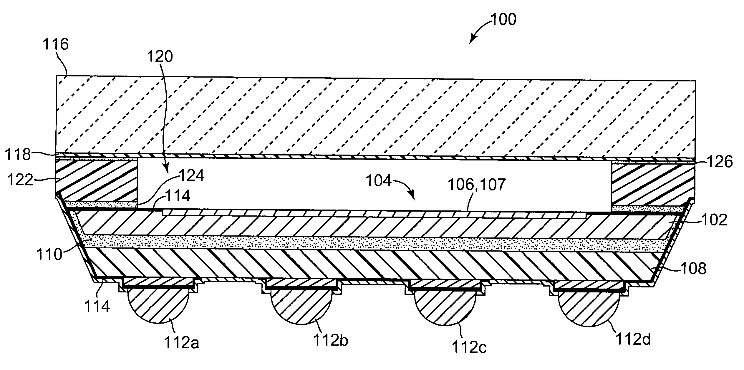
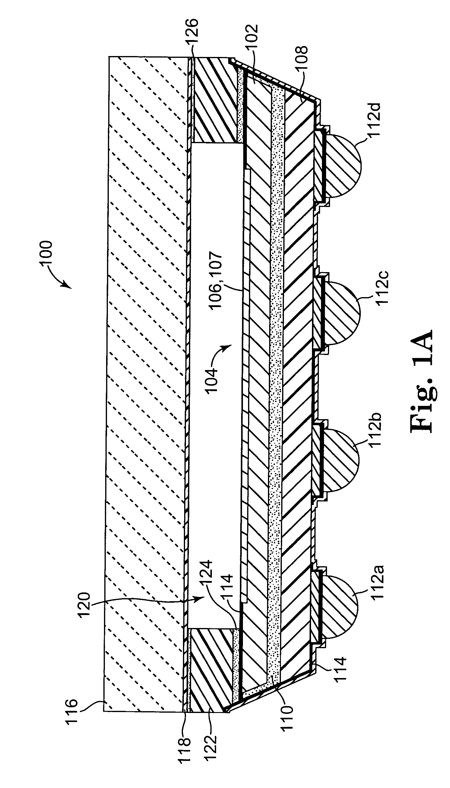
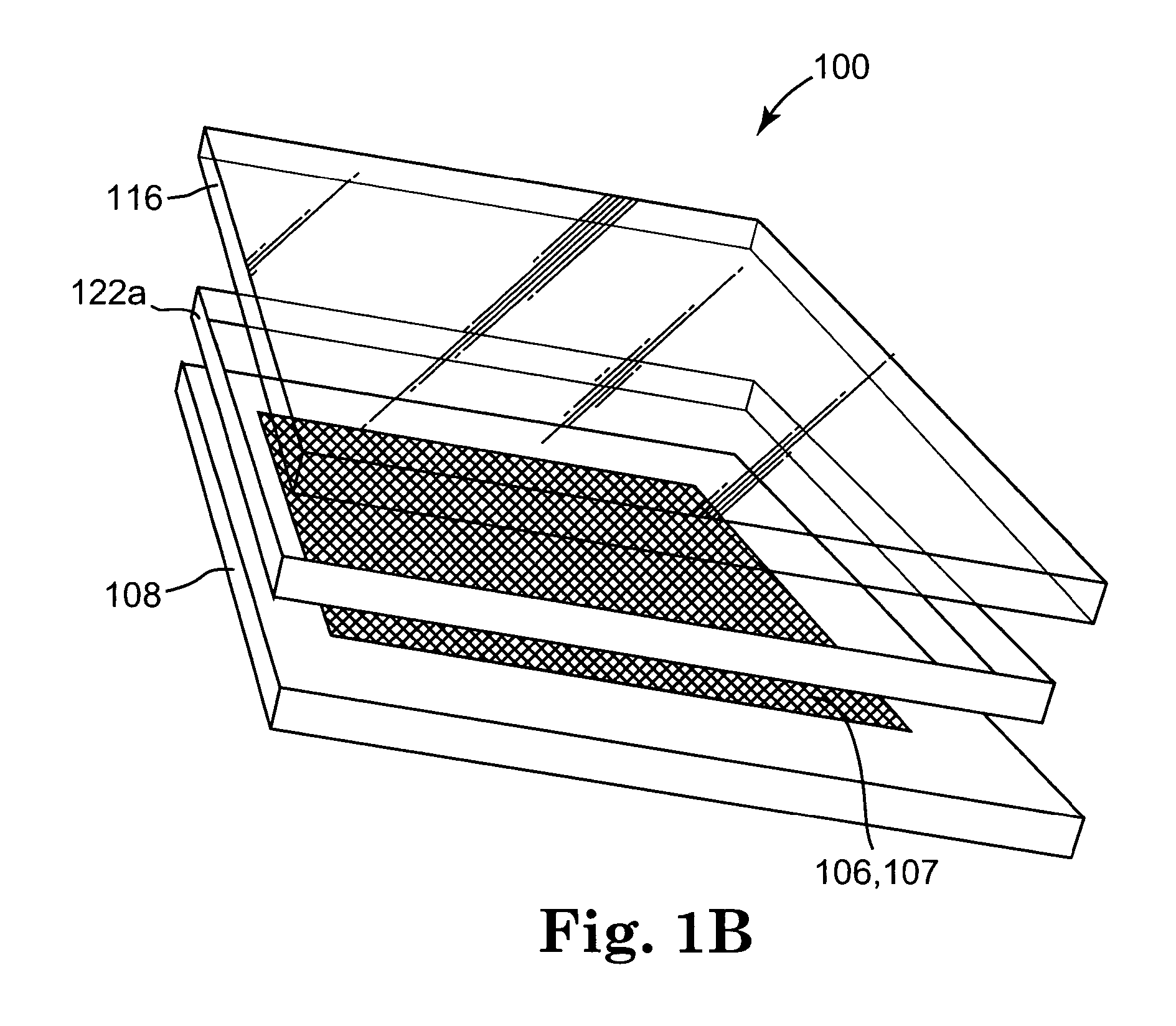
[0031]FIG. 1A illustrates an integrally-packaged imaging module 100 according to one aspect of the present invention. Imaging module 100 includes semiconductor substrate 102. In one embodiment, the surface of semiconductor substrate 102 includes an active area 104 containing integrated circuitry 106, which includes an image sensing device 107, an image processor, interface logic, and power conditioning circuitr...


PUM


Abstract

An integrally packaged imaging module includes an integrated circuit (IC), including an image sensing device formed on a semiconductor substrate, and wafer level packaging enclosing the IC. The wafer level packaging includes a transparent enclosure portion adapted to permit image acquisition of an image by the image sensing device over a desired range of wavelengths, and a first spacing structure providing a cavity between an inner surface of the transparent enclosure portion and the image sensing device. A depth of the cavity is configurable along an axis perpendicular to the semiconductor substrate to control a distance between an outer surface of the transparent enclosure portion and the image sensing device.

Description

THE FIELD OF THE INVENTION [0001] The present invention relates generally to imaging modules, and more particularly to an integrally-packaged imaging module. BACKGROUND OF THE INVENTION [0002] Digital imaging technology is being used in an increasing variety of mass-produced applications and in increasing production volumes. For example, miniature fixed-focus digital camera modules are being incorporated into end products such as portable telephones and personal digital assistants (PDA's). Given the new high volume applications for imaging modules, it is a continuing objective for imaging module fabricators to reduce their size and cost, and to provide imaging module designs that simplify incorporating the imaging modules into end products made by original equipment manufacturers (OEMs). [0003] Imaging modules generally include an image sensor that detects an image and converts it into an electrical signal representation. An image processor is employed to further manipulate the imag...

Claims


Application Information

Patent Timeline
IPC IPC(8): H01L31/0232H04N5/225
CPCH01L27/14618H01L27/14625H04N5/2257H04N5/2254H01L31/0232H01L2224/13H01L2224/05569H01L2224/05024H01L2224/05008H01L2224/05548H01L2224/05001H01L2924/00014H01L31/02325H01L2224/02377H01L24/05H04N23/57H04N23/55H01L2224/05599H01L2224/05099
Inventor MA, GUOLINAFSHARI, BAHRAM
Owner APTINA IMAGING CORP
Why Eureka
Try Eureka