Storage device with charge trapping structure and methods

a storage device and charge trapping technology, applied in the field of storage devices with charge trapping structure and methods, can solve the problems of affecting the reliability of the storage device, the processing speed is not high enough, and the storage capacity is typically achieved in a few hundred megabyte rang

Inactive Publication Date: 2005-04-21
HEWLETT PACKARD DEV CO LP
View PDF3 Cites 12 Cited by
  • Summary
  • Abstract
  • Description
  • Claims
  • Application Information

AI Technical Summary

Problems solved by technology

Solid state memory devices, typically, have read write speeds on the order of nanoseconds, however, storage capacities of only a few hundred Megabytes are typically achieved.
The ability to manufacture high capacity storage systems is typically constrained by the need to utilize movable or rotating parts, which is a relatively slow process compared to electronic circuit technology.
In addition, reliability is a further problem, in order to decrease the read write times the movable or rotating parts tend to be utilized at as high a speed as possible.
Further, if the electronic device is used in a portable application the shock resistance of the system is also typically a limitation.
Power consumption, overall weight and size, and cost also are factors that limit storage systems.
In turn, this increase in complexity has driven a corresponding decrease in the feature size of integrated circuit devices, which has typically followed “Moore's Law.” However, the continued decrease in feature size of integrated circuits, into the nanometer regime, has become increasingly more difficult, and may be approaching a limit, because of a combination of physical and economic reasons.
Generally, silicon based memory devices involve complex architectures utilizing many layers.
Each of these layers must be deposited and defined to produce the desired structure for that layer, thus each layer contributes to a higher cost for the semiconductor device.
In addition, such complex architectures, typically, result in a reduction in the number of logic cells per unit area of the semiconductor substrate, leading to a reduction in the data storage density for a given chip size.
As noted above it becomes increasingly difficult to squeeze more information into the storage devices.
If these problems persist, the continued growth, seen over the past several decades, in cheaper, higher speed, higher density, and lower power storage devices used in electronic devices will be impractical.

Method used


Image

  • Storage device with charge trapping structure and methods
  • Storage device with charge trapping structure and methods
  • Storage device with charge trapping structure and methods

Examples


Embodiment Construction

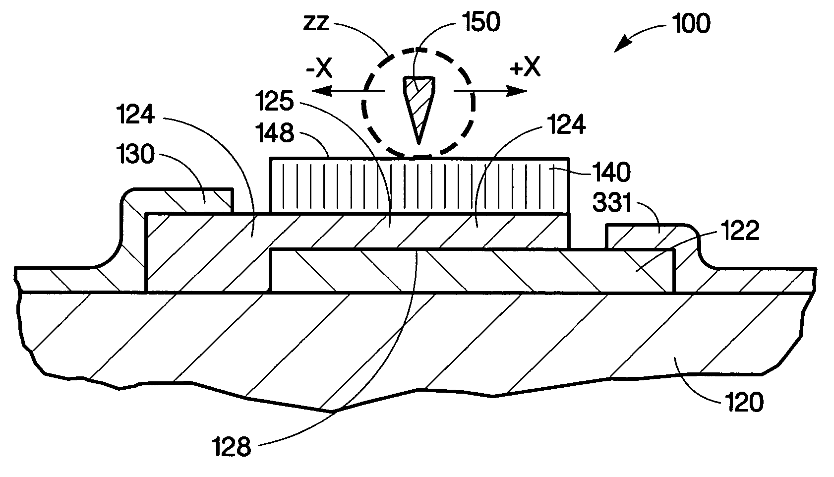
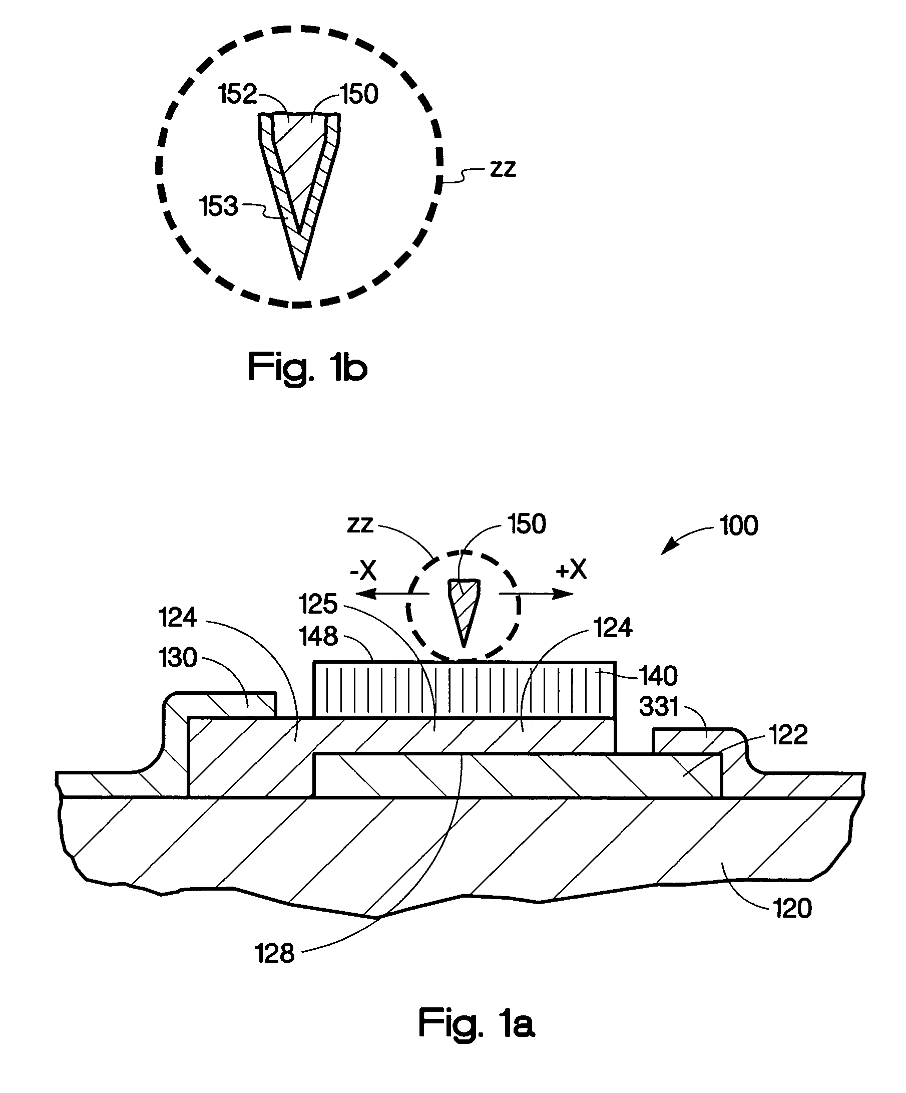
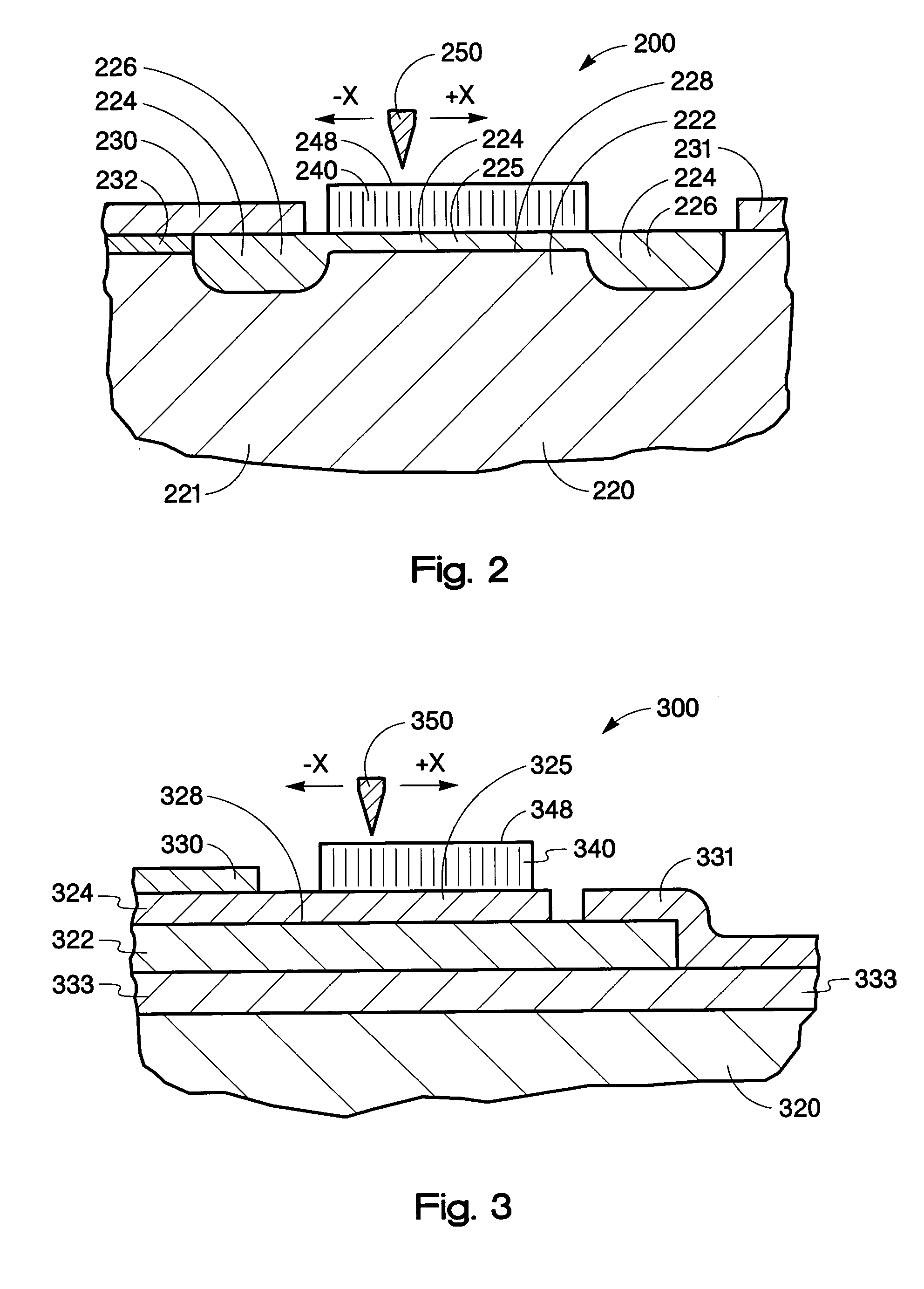
[0020] The present embodiments of this invention are directed to memory storage devices utilizing a charge trapping structure. The bit size of current solid state memory devices generally is limited by the dimensions capable of being resolved by the various photolithography technologies being utilized. The present invention utilizes a nano-scale conductive tip as a gate to control the localized charging and discharging of the charge trapping structure. In addition, in the present invention the nano-scale conductive tip and the charge trapping structure move relative to each other. The bit size of the present invention is not limited by photolithographic resolution but is generally determined by the size of the tip. Data may be read from and written to storage locations using the nano-scale conductive tip as a control gate. Accessing a specific storage location typically involves displacing the tip in either one or two dimensions.

[0021] An embodiment of memory storage device 100 of ...


PUM

PropertyMeasurementUnit
thicknessaaaaaaaaaa
thicknessaaaaaaaaaa
thicknessaaaaaaaaaa

Abstract

A storage device includes a first semiconducting layer having a p-dopant and a second semiconducting layer having an n-dopant, disposed on the first semiconducting layer forming a junction between the first and the second semiconducting layers. The storage device also includes a charge trapping structure disposed on the second semiconducting layer and a conductive gate, wherein the conductive gate and the charge trapping structure move relative to the other, wherein an electric field applied across the second semiconducting layer and the conductive gate traps charge in the charge trapping structure.

Description

DESCRIPTION OF THE ART [0001] Over the past few years, the demand for ever cheaper and lighter weight portable electronic devices has led to a growing need to manufacture durable, lightweight, and low cost electronic circuits including high density memory chips. Solid state memory devices, typically, have read write speeds on the order of nanoseconds, however, storage capacities of only a few hundred Megabytes are typically achieved. On the other hand, mass storage devices, which usually have a rotating medium, have the capability of storing multiple Gigabytes of data; however, they have read write speeds of the order of only milliseconds. [0002] The ability to manufacture high capacity storage systems is typically constrained by the need to utilize movable or rotating parts, which is a relatively slow process compared to electronic circuit technology. In addition, reliability is a further problem, in order to decrease the read write times the movable or rotating parts tend to be ut...

Claims


Application Information

Patent Timeline
Patent Type & Authority Applications(United States)
IPC IPC(8): H01L29/06G11B9/00G11B9/08G11B11/08H01L27/10
CPCB82Y10/00G11B9/08G11B9/14G11B11/08G11B9/1418G11B9/1436G11B9/1409
Inventor LIAO, HANGCHEN, ZHIZHANGGOVYADINOV, ALEXANDERSZEPESI, LESLIE LOUIS JR.LEE, HEON
Owner HEWLETT PACKARD DEV CO LP
Why Eureka
Try Eureka