Liquid crystal display panel and driving method therefor

Active Publication Date: 2005-04-21
HANNSTAR DISPLAY CORPORATION
View PDF1 Cites 35 Cited by
  • Summary
  • Abstract
  • Description
  • Claims
  • Application Information

AI Technical Summary

Benefits of technology

[0012] The first objective of the present invention is to provide a liquid crystal display panel. The polarity of a control electrode synchronously changes with the polarity of the pixel. When the polarity of the pixel is positive, the potential of the control electrode is higher than that of the pixel electrode; when the polarity of pixel is negative, the potential of control electrode is lower than that of the pixel electrode.
[0013] The second objective of the present invention is to provide a liquid crystal display panel, of which each pixel includes two thin film transistors. The thin film transistors are accompanied by driving signals to avoid the occurrence of a disclination line.
[0014] In order to achieve the objective, the present invention discloses a liquid crystal display panel and a driving method therfor, which includes an active matrix substrate having a plurality of thin film transistors. The active matrix substrat

Problems solved by technology

If we watch the display area from an oblique view angle, color distortion occurs in what we watch, and even gray inversion occurs.
However, because liquid crystal molecules are aligned in the same direction (mono-domain vertical alignment), we also cannot see a normal image from the view angle perpendicular to or symmetric to the direction.
But because the existence of the bumps results in that the precise alignment between a color filter and an active matrix substrate is necessary, and an additional over coating is necessarily formed on the color filter, the yield of this LCD panel becomes worse and the

Method used


Image

  • Liquid crystal display panel and driving method therefor
  • Liquid crystal display panel and driving method therefor
  • Liquid crystal display panel and driving method therefor

Examples


Example

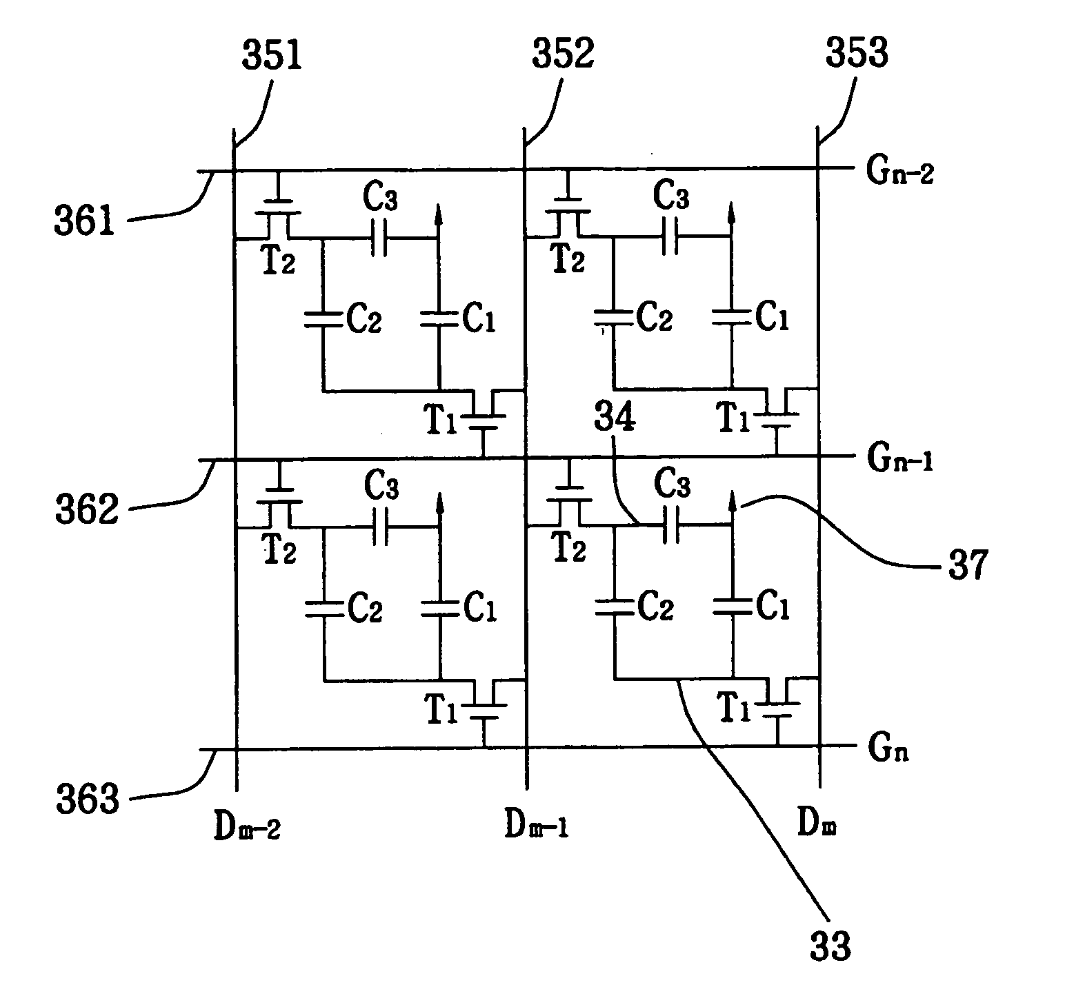
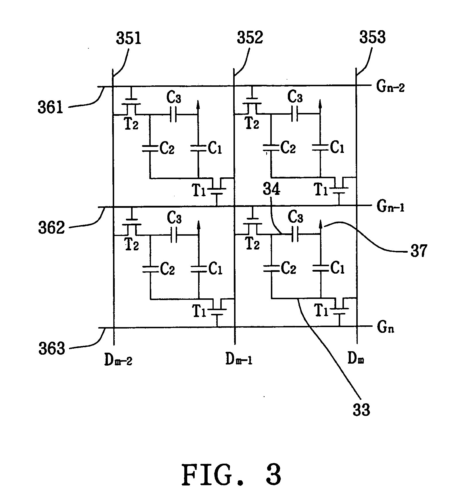
[0022]FIG. 3 an equivalent circuit diagram of the pixel of an LCD panel in accordance with the present invention. Only four adjacent pixels are shown in FIG. 3, which are formed by scanning lines 361, 362 and 363 (representing Gn-2, Gn-1 and Gn respectively) crossing data lines 351, 352 and 353 (representing Dm-2, Dm-1 and Dm respectively). Each pixel includes a first thin film transistor T1, a second thin film transistor T2, a control electrode 34 and a pixel electrode 33 for the pixel at the intersection of the data line 353 and scanning line 363. The first electrode of the first thin film thin film transistor T1 is connected to a data line 353, the second electrode of it is connected to the pixel electrode 33, and the gate electrode of it is connected to a scanning line 363. The first electrode of the second thin film transistor T2 is connected to another adjacent data line 352, the second electrode of it is connected to the control electrode 34, and the gate electrode of it is c...


PUM


Abstract

A liquid crystal display panel includes an active matrix substrate having a plurality of thin film transistors. The active matrix substrate comprises a plurality of parallel scanning lines and a plurality of parallel data lines, which cross mutually and form a plurality of pixels. Each of the pixels includes the first thin film transistor, the second thin film transistor, a control electrode (CE) and a pixel electrode. The first electrode of the first thin film transistor is connected to the data line; the second electrode of it is connected to the pixel electrode; the gate electrode of it is connected to the scanning line. The first electrode of the second thin film transistor is connected to another adjacent data line; the second electrode of it is connected to the control electrode, and the gate of it is connected to another adjacent scanning line. The scanning signals driving the pixel allows the control electrode and the pixel electrode to be written into their potentials during two horizontal scanning periods or during a vertical scanning period respectively.

Description

BACKGROUND OF THE INVENTION [0001] 1. Field of the Invention [0002] The prevented invention relates to a liquid crystal display panel and a driving method therefor, especially relates to a liquid crystal display panel and its driving method, which makes the potential of a control electrode higher than the potential of a pixel electrode by increasing the number of thin film transistors. [0003] 2. Description of the Related Art [0004] With the wide applications of liquid crystal display (LCD) panels, users have more and more demands about the quality of the LCD panel, such as high brightness, high contrast, high resolution, high color saturation and fast response time. Especially as the panel size increases, the LCD panels have generally been applied to household flat displays, such as liquid crystal (LC) TV sets, which have become an important application of the LCD panels. Most of the general, traditional LCD panels have narrow view angles so the normal images displayed by them only...

Claims


Application Information

Patent Timeline
IPC IPC(8): G02F1/136G09G3/36
CPCG09G3/3614G09G3/3655G09G2320/0223G09G2300/0809G09G2300/0876G09G3/3659
Inventor LEE, SEOK-LYULSHIH, PO-SHENG
Owner HANNSTAR DISPLAY CORPORATION
Why Eureka
Try Eureka