Chip scale package and method of fabricating the same

a technology of chip scale and scale package, which is applied in the direction of sustainable manufacturing/processing, final product manufacturing, electrical apparatus casing/cabinet/drawer, etc., can solve the problems of increasing the overall height of the package, increasing the production cost of the package, and the size of the substrate imposes a limit in miniaturizing the package, so as to improve the reliability of the package

Inactive Publication Date: 2005-04-28
SAMSUNG ELECTRO MECHANICS CO LTD
View PDF4 Cites 7 Cited by
  • Summary
  • Abstract
  • Description
  • Claims
  • Application Information

AI Technical Summary

Benefits of technology

[0013] Therefore, the present invention has been made in view of the above problems, and it is an object of the present invention to provide a chip scale package, which is miniaturized and more simply fabricated, by forming conductive layers on an upper and a lower surfaces of a chip with terminals and by forming electrode surfaces on side surfaces of the conductive layers, thereby improving the reliability of the package.

Problems solved by technology

However, these wires require a large space on the upper surface of the chip, thereby increasing the overall height of the package.
Therefore, the substrate has a large size so as to satisfy the aforementioned conditions, and the size of the substrate imposes a limit in miniaturizing the package.
Further, the ceramic substrate which is employed by the above-described package is high-priced, thereby increasing the production cost of the package.
Moreover, the conventional fabrication process of the package requires a wire-bonding step and a molding step as well as a die-bonding step, thereby being very complicated.

Method used


Image

  • Chip scale package and method of fabricating the same
  • Chip scale package and method of fabricating the same
  • Chip scale package and method of fabricating the same

Examples


Embodiment Construction

[0025] Now, preferred embodiments of the present invention will be described in detail with reference to the annexed drawings.

[0026]FIG. 3 is a perspective view of a chip scale package in accordance with a preferred embodiment of the present invention.

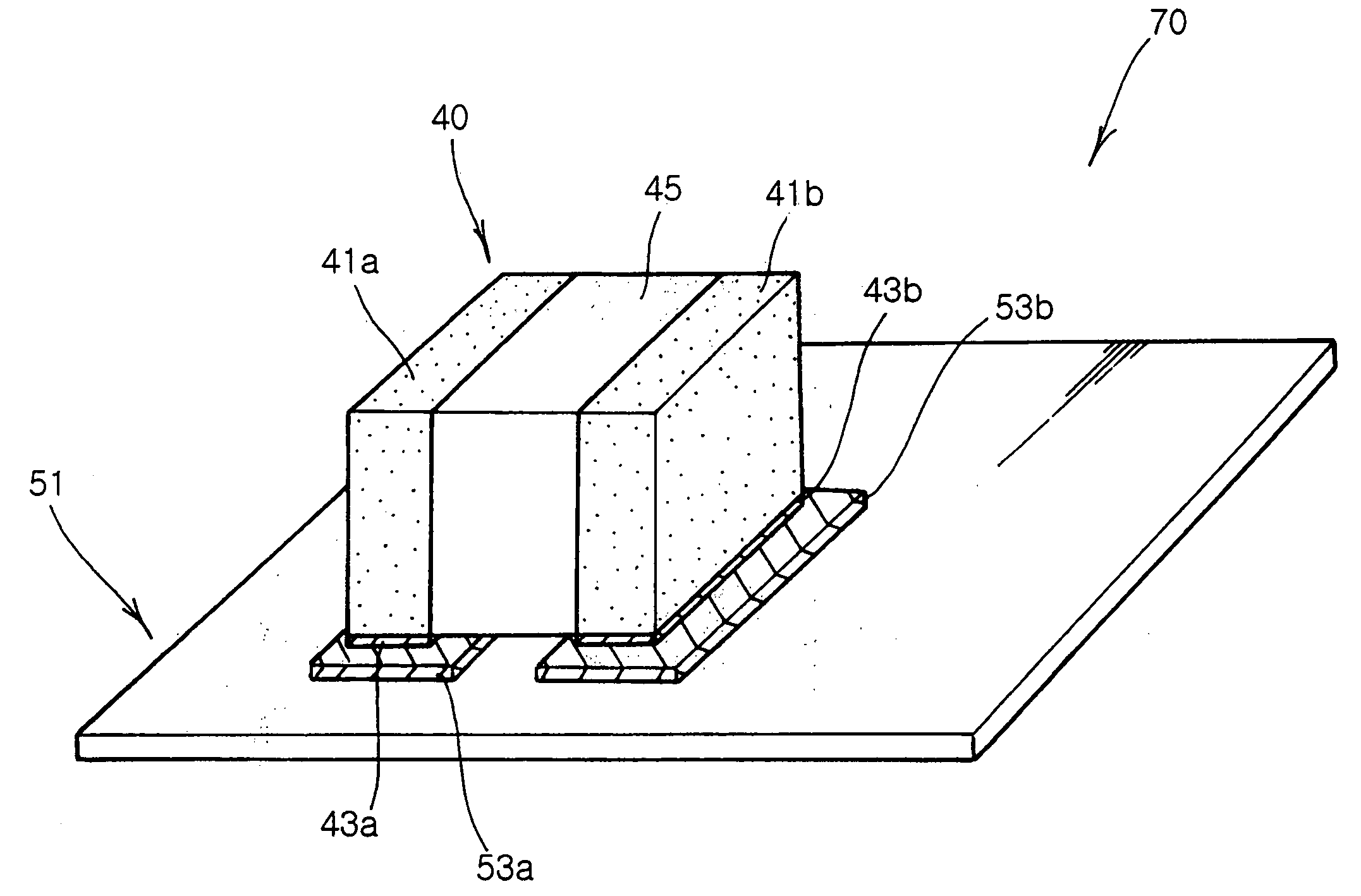
[0027] With reference to FIG. 3, a chip scale package 30 comprises a chip 35, an upper conductive layer 31a formed on the upper surface of the chip 35, a lower conductive layer 31b formed on the lower surface of the chip 35, a first electrode surface 33a formed on one side surface of the upper conductive layer 31a, and a second electrode surface 33b formed on one side surface of the lower conductive layer 31b. Herein, the side surface of the upper conductive layer 31a having the first electrode surface 33a and the side surface of the lower conductive layer 31b having the second electrode surface 33b are on the same side surface of the conductive layers 31a and 31b. The chip 35 includes an upper terminal (not shown) formed on the uppe...


PUM


Abstract

Disclosed are a chip scale package and a method of fabricating the chip scale package. The chip scale package comprises conductive layers with a designated depth formed on an upper and a lower surfaces of a chip, and electrode surfaces formed on the same side surfaces of the conductive layers, which are connected to corresponding connection pads of a printed circuit board. The chip scale package is miniaturized in the whole package size. Further, the method of fabricating the chip scale package does not require a wire-bonding step or a via hole forming step, thereby simplifying the fabrication process of the chip scale package and improving the reliability of the chip scale package.

Description

BACKGROUND OF THE INVENTION [0001] 1. Field of the Invention [0002] The present invention relates to a chip scale package, and more particularly to a chip scale package which is miniaturized and more easily fabricated by forming conductive layers on both surfaces of a chip and by forming electrode surfaces on side surfaces of the conductive layers, and a method of fabricating the chip scale package. [0003] 2. Description of the Related Art [0004] Generally, semiconductor devices such as diodes are packaged and these packaged devices are then mounted on a printed circuit board. Structurally, this package easily connects terminals of the semiconductor device to corresponding signal patterns of the printed circuit board and serves to protect the semiconductor device from external stresses, thereby improving reliability of the package. [0005] In order to satisfy recent trends of miniaturization of semiconductor products, the semiconductor chip packages also have been miniaturized. There...

Claims


Application Information

Patent Timeline
Patent Type & Authority Applications(United States)
IPC IPC(8): H01L23/12H01L21/60H01L21/78H01L23/31H01L23/48H01L23/485H05K3/34H05K5/00
CPCH01L21/78H01L23/3114H01L2924/00014H01L2224/32225H01L24/48H01L24/05H05K2201/10636H05K2201/09381H05K5/0091H05K3/3442H01L2924/014H01L2924/01079H01L2924/01078H01L2924/01033H01L2924/01029H01L2924/01015H01L2924/01014H01L2924/01006H01L2924/01005H01L2924/01004H01L2224/97H01L2224/85399H01L24/97H01L2224/04042H01L2224/05599H01L2224/48091H01L2224/48227H01L2224/48235H01L2224/4848H01L2224/73265H01L2224/85051H01L2224/45099H01L2924/00H01L2924/15787H01L2924/181Y02P70/50H01L2924/00012H01L23/48
Inventor YOON, JOON HOCHOI, YONG CHILBAE, SUK SU
Owner SAMSUNG ELECTRO MECHANICS CO LTD
Why Eureka
Try Eureka