Capacitive load driver and plasma display

a capacitive load and driver technology, applied in static indicating devices, cathode-ray tube indicators, instruments, etc., can solve the problems of screen upsizing, increased reactive power of screen devices, and hindered slimming-down and miniaturization, so as to reduce the total power consumption of the system including the load, reduce the reactive power, and avoid adverse effects on the other circuit parts

Inactive Publication Date: 2005-04-28
PANASONIC CORP
View PDF1 Cites 32 Cited by
  • Summary
  • Abstract
  • Description
  • Claims
  • Application Information

AI Technical Summary

Benefits of technology

[0024] An object of the present invention is to provide a driver of a capacitive load like a PDP; the driver can effectively suppress the reactive power caused by the charging and discharging of the capacitive load, using a smaller number of its components than those of a conventional driver and avoiding adverse effects on the other circuit parts, and can further reduce the total power consumptions of the system including the load.

Problems solved by technology

The charging and discharging currents cause power consumption at resistances of the circuit devices of the PDP driver, the sustain and scan electrodes of the PDP, and the lead wires.
However, the screen upsizing increases the reactive power caused by the charging and discharging of the panel capacitance.
Thus, the slimming-down and miniaturization are hindered.

Method used


Image

  • Capacitive load driver and plasma display
  • Capacitive load driver and plasma display
  • Capacitive load driver and plasma display

Examples


embodiment 1

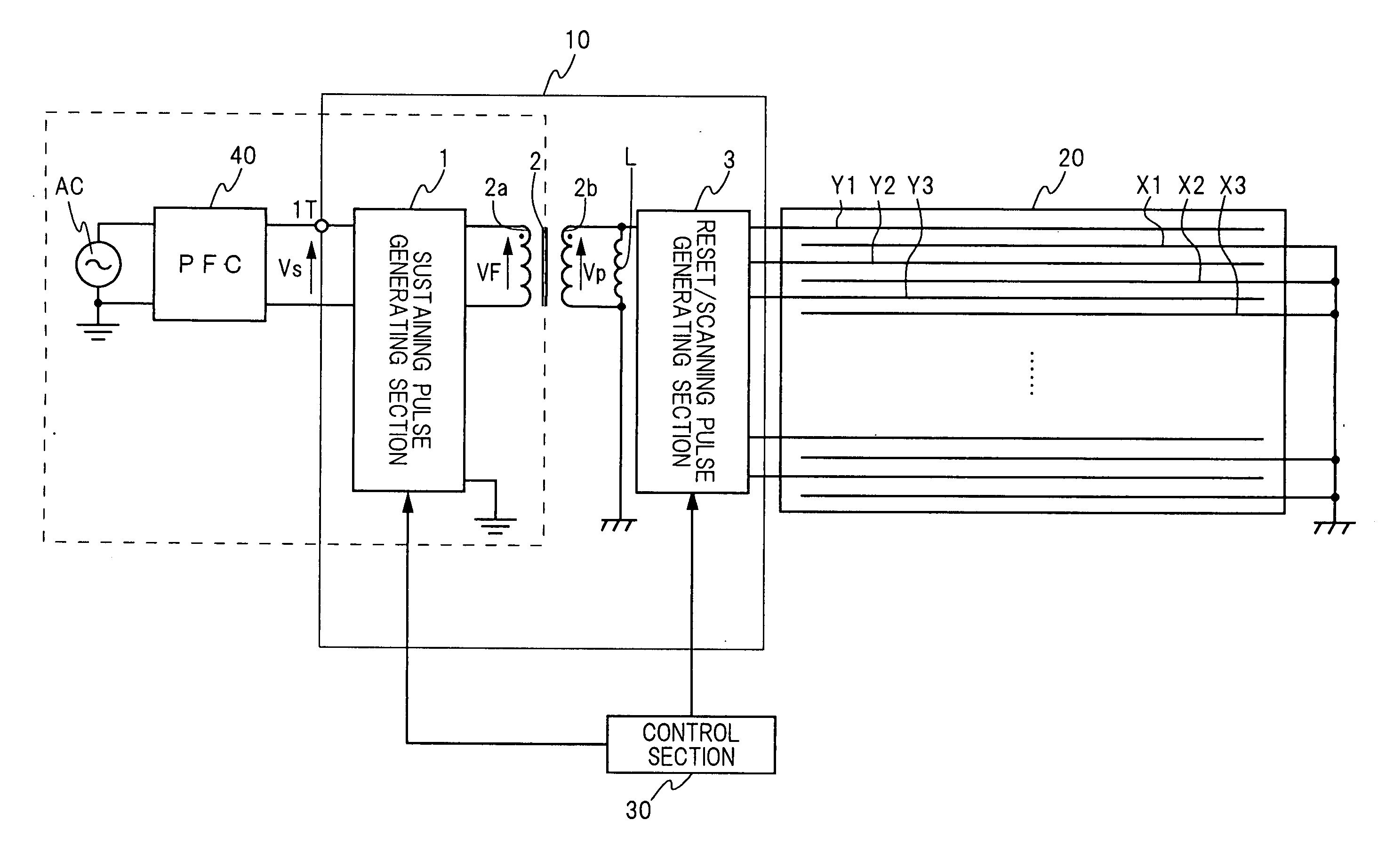
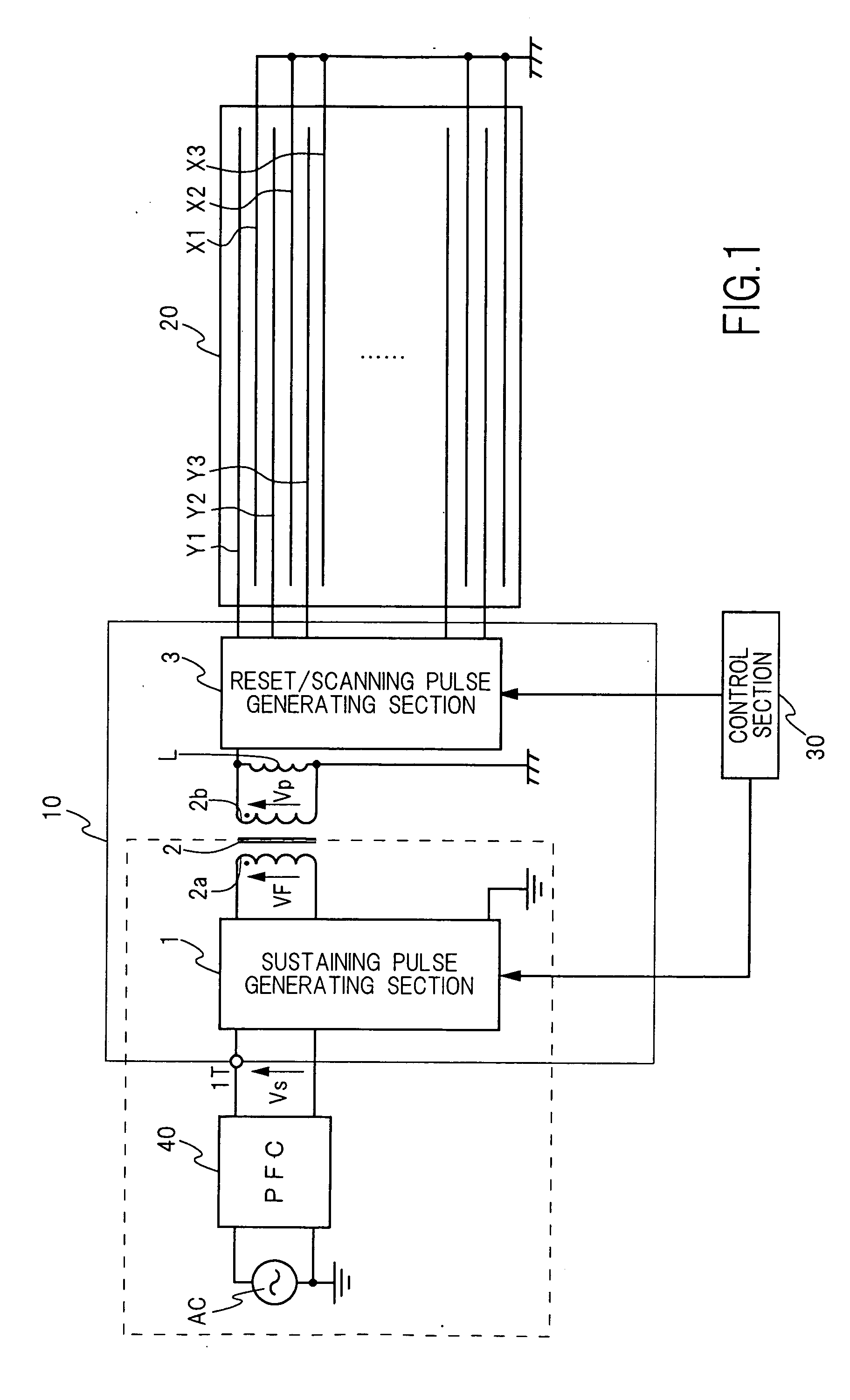
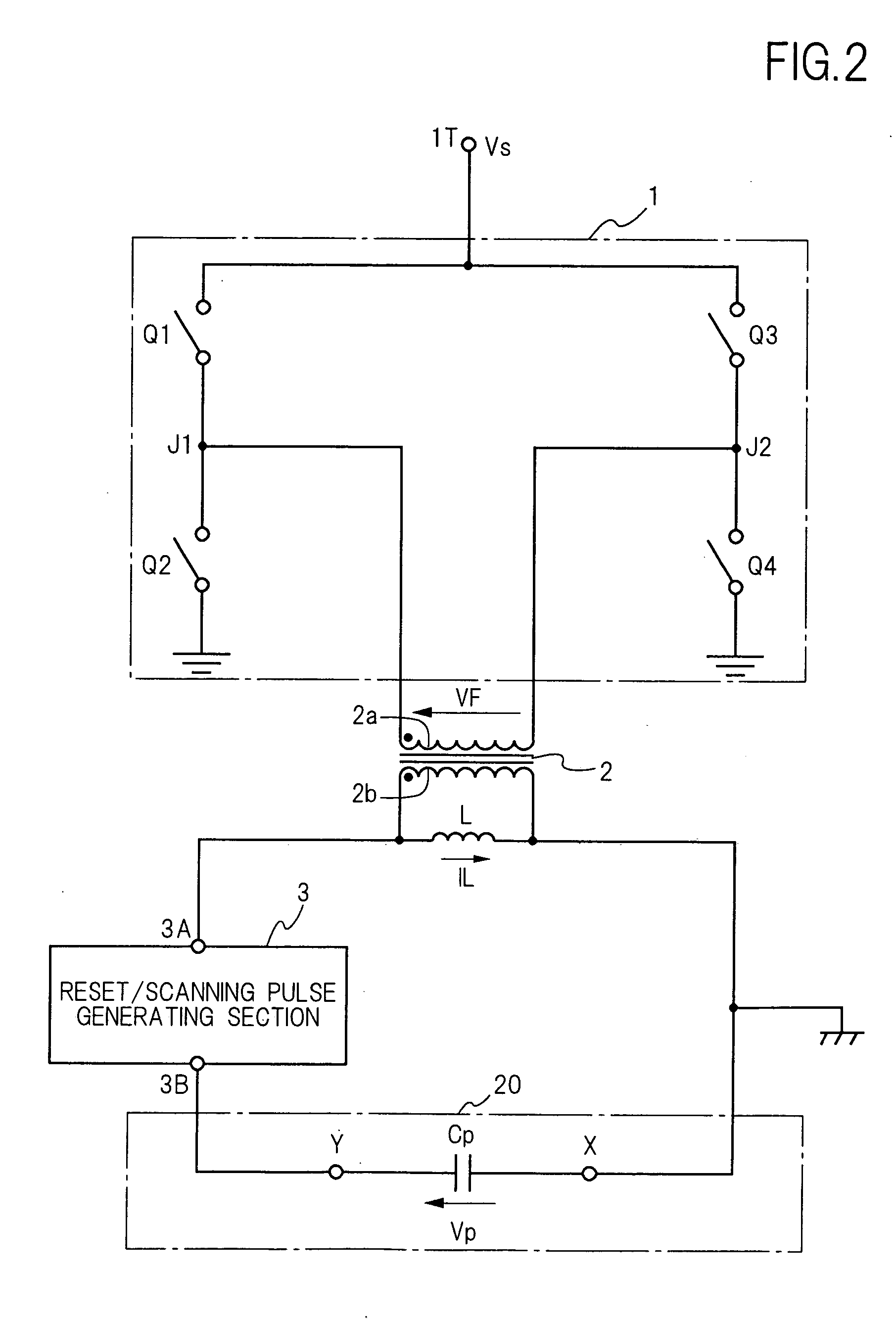
[0124]FIG. 1 is the block diagram which shows the configuration of the plasma display according to Embodiment 1 of the invention.

[0125] The plasma display comprises a PDP 20, a PFC converter 40, a PDP driver 10, and a control section 30.

[0126] The PDP 20 is preferably an AC type and comprises a three-electrode surface-discharge type structure. Address electrodes (not shown) are arranged on the rear substrate of the PDP 20 in the vertical direction of the panel. Sustain electrodes X1, X2, X3, . . . and scan electrodes Y1, Y2, Y3, . . . are alternately arranged on the front substrate of the PDP 20 in the horizontal direction of the panel. The sustain electrodes X1, X2, X3, . . . , are connected to each other, and thereby, maintained at a substantially equal potential. The address electrodes and the scan electrodes Y1, Y2, Y3, . . . each allow the separate potential changes.

[0127] A discharge cell (not shown) is installed at the intersection of a pair of sustain and scan electrodes ...

embodiment 2

[0193]FIG. 6 is the block diagram which shows the configuration of the plasma display according to Embodiment 2 of the invention. In FIG. 6, the components similar to the components shown in FIG. 1 are marked with the same reference symbols as the reference symbols shown in FIG. 1. Furthermore, for the details of the similar components, the explanation about Embodiment 1 is cited.

[0194] This plasma display comprises a PFC converter 40, a PDP driver, a PDP 20, and a control section 31. The PDP driver includes a first driver section 10Y and a second driver section 10X.

[0195] The first driver section 10Y includes a first sustaining pulse generating section 1Y, a first transformer 2Y, a first inductor LY, and a reset / scanning pulse generating section 3Y. The second driver section 10X includes a second sustaining pulse generating section 1X, a second transformer 2X, a second inductor LX, and a reset pulse generating section 3X. Here, the reset pulse generating section may be included o...

embodiment 3

[0234]FIG. 10 is the block diagram which shows the configuration of plasma display according to Embodiment 3 of the invention. In FIG. 10, the components similar to the components shown in FIG. 1 are marked with the same reference symbols as the reference symbols shown in FIG. 1. Furthermore, for the details of the similar components, the explanation about Embodiment 1 is cited.

[0235] This plasma display comprises a PFC converter 40, a PDP driver, a PDP 20, and a control section 32. The PDP driver includes a first driver section 10A, a second driver section 10B, and a reset / scanning pulse generating section 3. The first driver section 10A includes a first sustaining pulse generating section 1A, a first transformer 2A, and a first inductor LA. The second driver section 10Ba includes a second sustaining pulse generating section 1B, a second transformer 2B, and a second inductor LB.

[0236] In this plasma display, each of the secondary windings 2bA and 2bB of the two transformers 2A an...


PUM


Abstract

Sustain electrodes (X1, X2, . . . ) of a PDP (20) are grounded. A PFC converter (40) converts an alternating voltage into a DC voltage (Vs) and applies it directly across a PDP driver (10). A sustaining pulse generating section (1) converts the DC voltage (Vs) into a primary voltage pulse (VF), and applies it across a primary winding (2a) of a transformer (2). The transformer (2) converts the primary voltage pulse (VF) into a sustaining voltage pulse (Vp), and applies it to scan electrodes (Y1, Y2, . . . ) of the PDP (20) through a reset / scanning pulse generating section (3). An inductor (L) is connected in parallel with a secondary winding (2b) of the transformer (2). The inductor (L) resonates with the panel capacitance of the PDP (20) at the rising and falling edges of the sustain voltage pulse (Vp).

Description

BACKGROUND OF THE INVENTION [0001] The present invention relates to a driver for a capacitive load such as a plasma display panel (PDP). [0002] A plasma display is a display device that uses a luminous phenomenon caused by gas electric discharge. A plasma display panel (PDP) has advantages in upsizing the screen, slimming down, and widening the viewing angle over other display devices. PDPs are broadly classified into two types; a DC type which works by DC pulses, and an AC type which works by AC pulses. The AC-type PDPs has, in particular, a higher brightness and a simpler structure. Accordingly, the AC-type PDPs are suitable for mass production and increase in pixel density, thereby coming into extensive use. [0003]FIG. 42 is a block diagram that shows a configuration of a conventional plasma display. See for example, Published Japanese patent application Hei 5-191977 gazette, U.S. Pat. No. 4,866,349, and Published Japanese patent application Hei 11-344952 gazette. The conventiona...

Claims


Application Information

Patent Timeline
Patent Type & Authority Applications(United States)
IPC IPC(8): G09G3/28G09G3/288G09G5/00
CPCG09G3/2927G09G2330/02G09G3/2965
Inventor INOUE, MANABUYOSHIDA, KOJIIKEDA, SATOSHIARAI, YASUHIRO
Owner PANASONIC CORP
Why Eureka
Try Eureka