Image display device and driving method thereof

a technology of image display and driving method, which is applied in the direction of lighting apparatus, instruments, light sources, etc., can solve the problems of poor display, deterioration of image quality, and possible result of display deterioration, so as to improve writing performance and suppress power consumption

Inactive Publication Date: 2005-03-29
SHARP KK
View PDF11 Cites 25 Cited by
  • Summary
  • Abstract
  • Description
  • Claims
  • Application Information

AI Technical Summary

Benefits of technology

In view of the foregoing problems, it is an object of the present invention to provide an image display device having a pre-charging function to (i) suppress an increase of power consumption, and to (ii) particularly improve a writing performance of writing a video signal into a data signal line, and a driving method of such an image display device.
In the present invention, the pre-charging voltage stabilizing circuit having charge holding means and current controlling means is adopted as the pre-charging voltage stabilizing means, and when performing black display in an upper black display area and a lower black display area which are respectively provided in the upper and lower parts of the screen of the display section, by a pre-charging voltage from the pre-charging circuit, a scanning signal is suspended for a predetermined period of time, thereby supplying a scanning signal after sufficiently storing charges in the charge holding means of the pre-charging voltage stabilizing circuit, charging a pixel to the equivalent of a black display voltage, suppressing fluctuation in the pre-charging voltage in an area to display a video signal, and charging each data signal line to a desired voltage, thus suppressing impairment of an image quality of the image display device.

Problems solved by technology

This, however, involves a problem of considerable deterioration of image quality caused by the video signal DAT which was incompletely written into the data signal line SL due to the higher sampling rate.
As a result, this may adversely affect a voltage of the video signal DAT to be written into the data signal line SL by the data signal line driving circuit SD, thus, deterioration of display may be resulted therefrom.
Furthermore, an abrupt change in the pre-charging voltage PCV may trigger power fluctuation, which causes all of the control signals to become unstable, thereby possibly resulting in poor display.
However, this raises a new problem of increasing power consumption due to the current amplifying section thus provided.
However, nowadays, the screen of a TV which is larger in the width than the height (“wide TV”, hereinafter) has been the mainstream of home TVs, and when displaying a picture recorded by the video camcorder on this wide TV, upper and lower parts of the picture are lost.
However, in the foregoing image display device, though provision of the current amplifying section Buffer enables stable supply of the pre-charging voltage PCV, yet there arises a problem that the current amplifying section Buffer increases power consumption.

Method used


Image

  • Image display device and driving method thereof
  • Image display device and driving method thereof
  • Image display device and driving method thereof

Examples


first embodiment

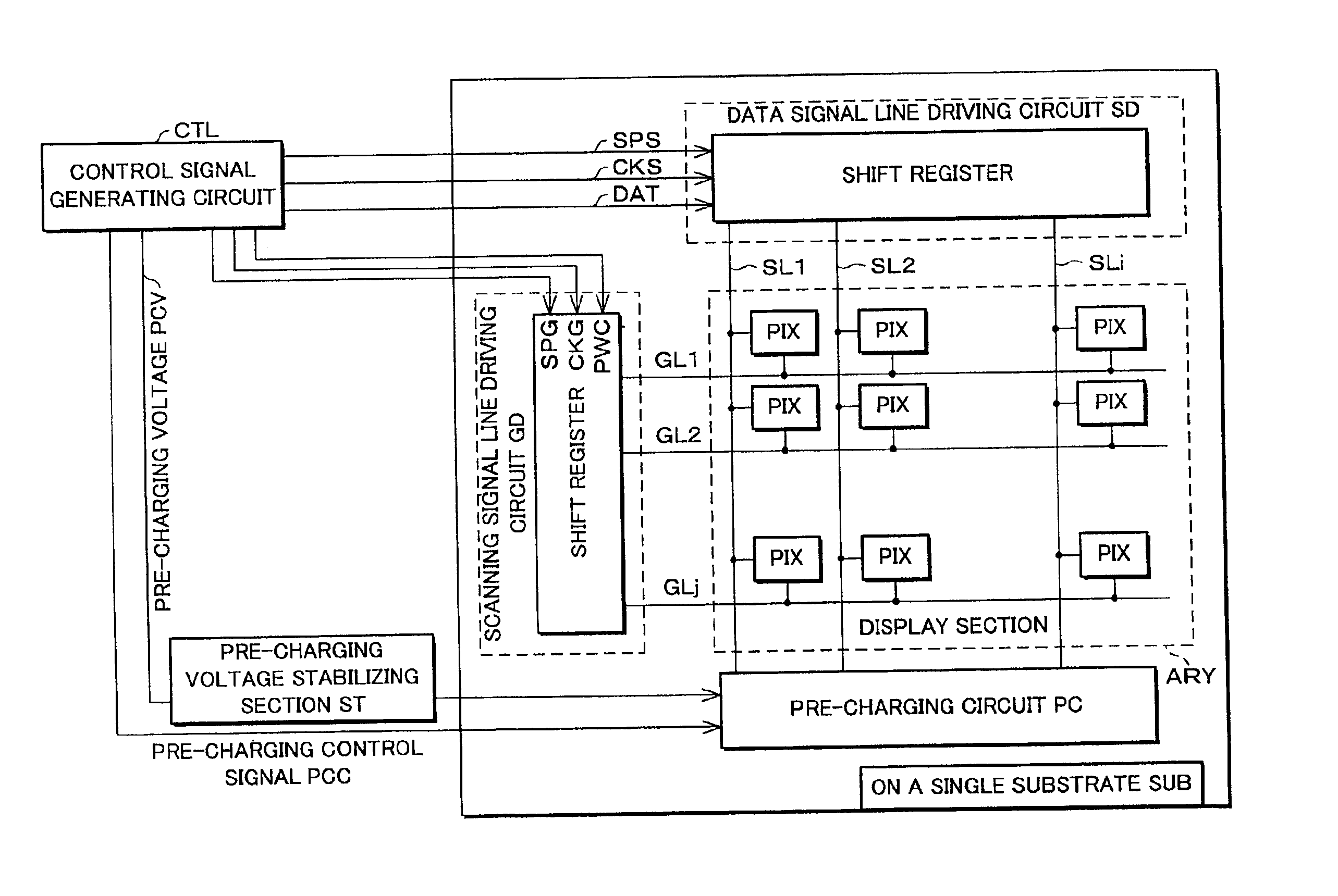
The following will explain a First Embodiment according to the present invention with reference to drawings. FIG. 1 is a block diagram showing one example of a structure of an image display device.

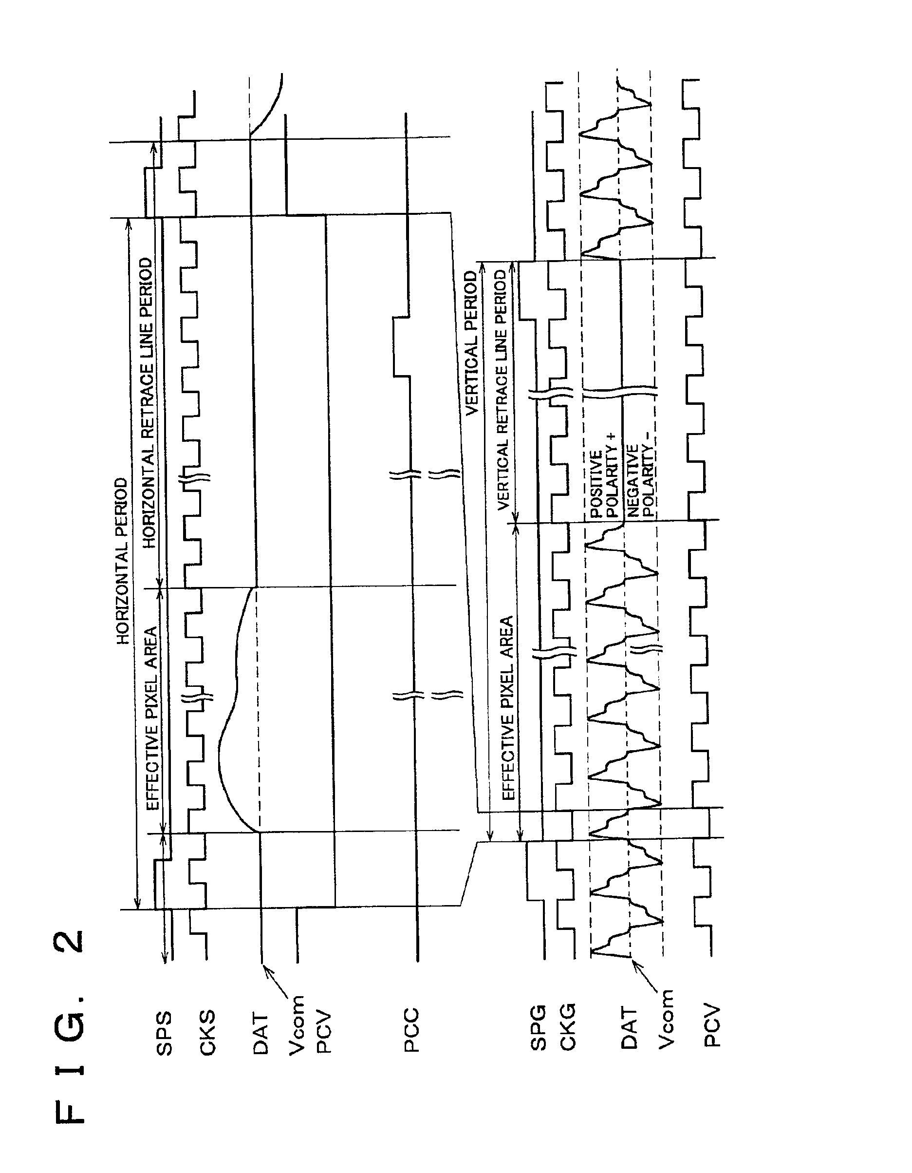
As shown in FIG. 1, the image display device according to the present invention is made up of: a data signal line driving circuit SD; a scanning signal line driving circuit GD; a data signal line SLi (i≧1); a scanning signal line GLj (j≧1); a pixel PIX; a control signal generating circuit CTL; a pre-charging circuit PC; and a pre-charging voltage stabilizing section ST. The control signal generating circuit CTL outputs each control signal in a manner shown in a timing chart of FIG. 2.

In addition, respective switching elements of the data signal line driving circuit SD, scanning signal line driving circuit GD, pre-charging circuit PC and each pixel PIX are made from a polycrystalline silicon thin film transistor at a process temperature of not more than 600° C. on a single substrate SUB.

Fur...

second embodiment

Here, the DC voltage is given to the pre-charging voltage PCV, and in the Second Embodiment, the pre-charging voltage PCV is set to be equipotential from the maximum amplification values of positive and negative polarities of the video signal DAT, respectively. That is, in FIG. 2, the polarity of the counter voltage Vcom is changed for every horizontal period (1H), and the counter voltage Vcom becomes a reference to positive or negative polarity. The potential difference between the counter voltage Vcom and the maximum amplification value of the positive polarity, and the potential difference between the counter voltage Vcom and the maximum amplification value of the negative polarity are set to be equal (equipotential).

Further, in the Second Embodiment, the driving method called 1H reversal driving is also adopted, by which the polarity of the video signal DAT to be written into pixel PIX is switched between positive and negative for every horizontal period.

Next, the following will...

third embodiment

Here, the present invention will be explained. The image display device shown in FIG. 12 is made up of a data signal line driving circuit SD, a scanning signal line driving circuit GD, a pixel array ARY, a control signal generating circuit CTL, a pre-charging circuit PC, and a pre-charging voltage stabilizing circuit ST, wherein each pixel PIX which forms the pixel array ARY is connected with a data signal line SDLi (i=1 to m) and a scanning signal line GLj (j=1 to n), respectively. Further, as discussed later, the pixel PIX, the data signal line driving circuit SD, the scanning signal line driving circuit GD and the pre-charging circuit PC are formed on a single substrate SUB.

As shown in FIG. 16, the control signal generating circuit CTL includes a counter CNT for counting a reference clock (CLK), a plurality of pairs of comparators CPR in which a timing of normal display and a timing in a wide mode are respectively set, and a selector ST for selecting output of the plurality of co...


PUM


Abstract

An image display device of this invention includes a pre-charging voltage stabilizing section having current controlling means and charge holding means which respectively include a resistor and a capacitor to stabilize a pre-charging voltage. The charge holding means holds a voltage to be supplied to data signal lines, and the current controlling means suppresses a current flow from a control signal generating circuit, thereby suppressing power fluctuation at the control signal generating circuit. This suppresses fluctuation in the pre-charging voltage and enables data signal lines to be charged to a predetermined voltage, thereby suppressing deterioration of image quality and an increase in power consumption of the image display device. Further, when using the pre-charging voltage stabilizing section and setting a portion of a display as a video data non-display area avoiding display of video data in a non-match image display mode to display at fixed brightness in the video data non-display area by a pre-charging voltage from a pre-charging circuit, a control signal is suspended in a fixed period, thus realizing a non-match image display mode to display a video image of an aspect ratio different from that of a screen of a display without impairing an image quality, and saving power.

Description

FIELD OF THE INVENTIONThe present invention relates to an image display device and a driving method thereof, and in particular to an image display device having a pre-charging function to stabilize a state of data signal lines which are successively scanned by a data signal line driving circuit and to improve a writing performance of a video signal, and a driving method thereof. Further, the present invention relates to an image display device having a non-match image display mode which enables display of a video image, an aspect ratio of which differs from that of a screen of a display device, and a driving method thereof.BACKGROUND OF THE INVENTIONThe following will explain one example of a conventional image display device, i.e. an active matrix type liquid crystal display device. As shown in FIG. 9, this image display device is made up of a pixel array ARY, a scanning signal line driving circuit GD, a data signal line driving circuit SD and a pre-charging circuit PC.The pixel ar...

Claims


Application Information

Patent Timeline
Patent Type & Authority Patents(United States)
IPC IPC(8): G09G3/36
CPCG09G3/3685G09G3/3696G09G3/3614G09G2330/021G09G2310/0232G09G2310/0251
Inventor WASHIO, HAJIMEKUWABARA, NOBUHIROYONEDA, HIROSHIYOSHIDA, SHIGETO
Owner SHARP KK
Why Eureka
Try Eureka