
IPS liquid crystal display device

Active Publication Date: 2005-04-28
BEIHAI HKC OPTOELECTRONICS TECH CO LTD
View PDF6 Cites 21 Cited by
  • Summary
  • Abstract
  • Description
  • Claims
  • Application Information

AI Technical Summary

Benefits of technology

[0015] The present invention has been achieved to solve the foregoing problems and it is therefore an object of the present invention to reduce optical leakage from the outer peripheral portion (edge portion) of a tilted electrode pattern and thereby improve contrast in an IPS liquid crystal display device having a flexed electrode pattern structure.
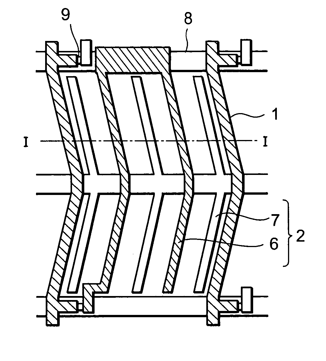
[0019] In the conventional IPS liquid crystal display device, the electrode pattern which is not orthogonal or parallel to the optical axis had the problem that the outer peripheral portion thereof generates a polarized light component which is not absorbed by the analyzer as a result of diffraction and thereby increases the dark brightness. By contrast, the foregoing electrode pattern structure according to the present invention shuts off the diffracted light at each of the stepped portions, eliminates optical leakage from the outer peripheral portion of the electrode-pattern, and thereby improves the contrast of display on a screen.

Problems solved by technology

Thus, the IPS liquid crystal display device has the advantage of the extremely wide viewing angle, while having the disadvantage that a screen is tinted in a yellow or blue color when viewed in a tilted fashion from the longitudinal direction of the electrodes in the comb-like configuration.
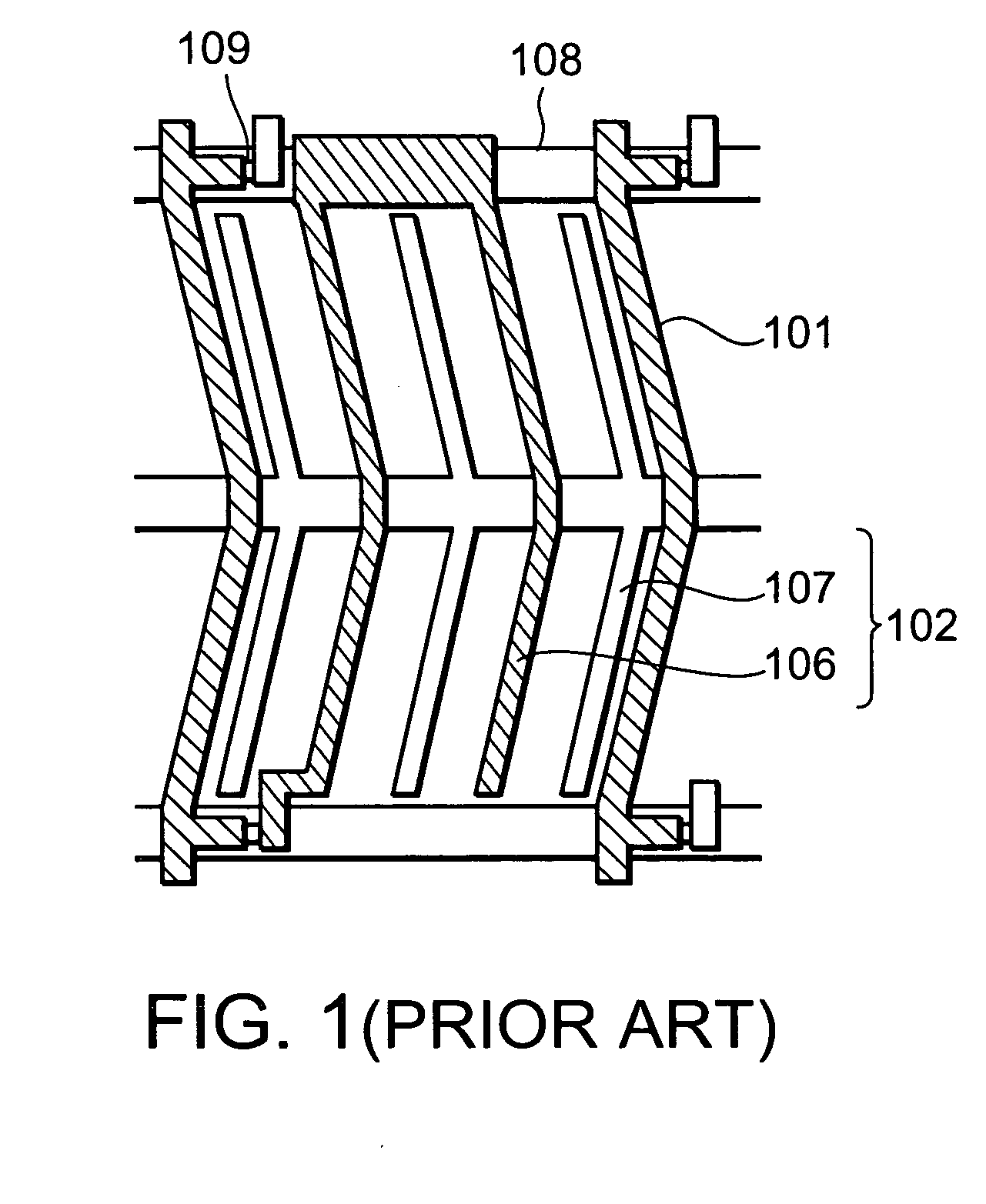
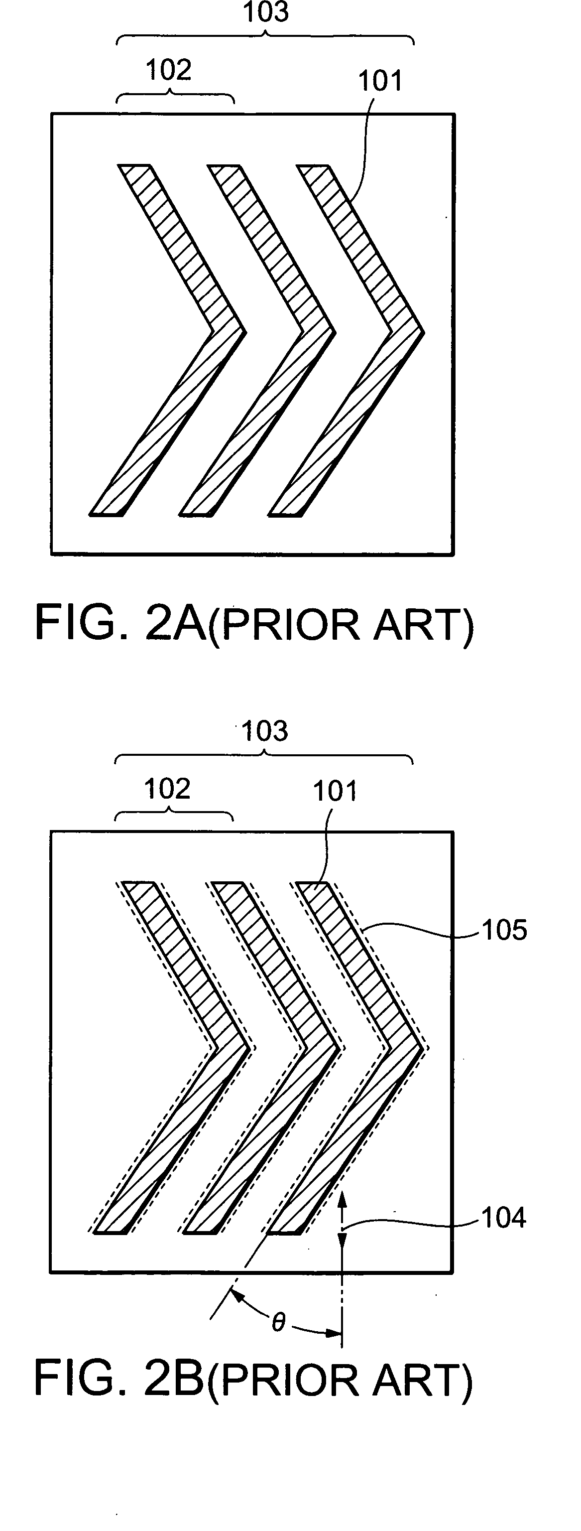
Consequently, diffracted light having a polarized light component which is not absorbed by an analyzer (polarizer plate) is generated by the outer peripheral portion (edge portion), so that optical leakage occurs.
Thus, the liquid crystal display device has the problem that the optical leakage increases dark brightness and degrades contrast.
As a result, dark brightness increases and contrast deteriorates.
Thus, the metal electrode which is not orthogonal or parallel to the optical axis 104 has the problem that the outer peripheral portion thereof generates a polarized light component which is not absorbed by the analyzer as a result of diffraction and increases the dark brightness.

Method used


Image

  • IPS liquid crystal display device
  • IPS liquid crystal display device
  • IPS liquid crystal display device

Examples


Embodiment Construction

[0029] Referring to the drawings, the embodiments of the present invention will be described herein below. FIG. 4A is a plan view diagrammatically showing the pixel region of an IPS liquid crystal display device having an electrode pattern structure according to the present invention. FIG. 4B is a sectional view of a liquid crystal display panel taken along line I-I of FIG. 4A.

[0030]FIG. 5 is an enlarged plan view of the electrode pattern in the pixel region of FIG. 4A.

[0031] As shown in FIG. 4A and FIG. 4B, the IPS liquid crystal display device according to the present invention comprises a plurality of signal lines 1 and scan lines 8 arranged as a matrix on a first substrate 20. TFT switching elements 9 are provided at the individual points of intersection of the signal lines 1 and the scan lines 8 on the first substrate. Comb-like pixel electrodes 6 and a comb-like common electrode 7 are connected to the TFT switching elements 9. The pixel electrodes 6 and the common electrode ...


PUM


Abstract

In an IPS liquid crystal display device, a reduction in optical leakage from the outer peripheral portion (edge portion) of an electrode pattern in flexed configuration and an improvement in the contrast of display on a screen are intended. An IPS liquid crystal display device of the present invention has a plurality of signal lines and scan lines arranged as a matrix on a TFT substrate, TFT switching elements, and comb-like pixel electrodes connected to the TFT switching elements. In a pixel region, a comb-like common electrode is formed in interdigitated relation with the pixel electrodes. The pixel electrodes, the common electrode, and the signal lines are formed in mutually parallel and flexed configuration at a given angle relative to an optical axis. The outer edge of each of the pixel electrodes, the common electrode, and the signal lines is added with fine stairwise fine stepped portions composed of the same material as composing the electrodes and lines. The stepped portions prevent optical leakage from the outer peripheral portion of the flexed electrode pattern.

Description

BACKGROUND OF THE INVENTION [0001] 1. Field of the Invention [0002] The present invention relates to an IPS (In-Plane Switching) liquid crystal display device and, more particularly, to a pattern structure of electrodes and wiring in the pixel region of the IPS liquid crystal display device. [0003] 2. Description of the Prior Art [0004] In an IPS liquid crystal display device, a liquid crystal is sealed in a space between a pair of transparent substrates and an electric field substantially parallel to a surface of one of these substrates is applied thereto, whereby liquid crystal molecules are rotated and oriented in a direction horizontal to the substrate surface. The IPS liquid crystal display device can achieve a wide viewing angle by orienting the liquid crystal molecules in a direction horizontal to the substrate surface. [0005] Pixel electrodes and a common electrode which are formed at a given spacing are arranged in a comb-like configuration on the transparent substrate to w...

Claims


Application Information

Patent Timeline
IPC IPC(8): G02F1/133G02F1/1335G02F1/1343G02F1/136H01L29/786
CPCG02F2201/122G02F1/134363G02F1/1343
Inventor MIZOGUCHI, CHIKAAKI
Owner BEIHAI HKC OPTOELECTRONICS TECH CO LTD
Learn More