Self-patterning of photo-active dielectric materials for interconnect isolation

a dielectric material and self-patterning technology, applied in the manufacturing of solid-state devices, electric devices, semiconductor/solid-state devices, etc., can solve the problems of high increased cost of creating conductive interconnect patterns, and potential contamination of low-k dielectric materials

Inactive Publication Date: 2005-05-05
CHARTERED SEMICONDUCTOR MANUFACTURING
View PDF6 Cites 49 Cited by
  • Summary
  • Abstract
  • Description
  • Claims
  • Application Information

AI Technical Summary

Benefits of technology

[0016] A principal objective of the invention is to provide a method of creating interconnect patterns that does not require the creation of an overlying photoresist exposure mask.
[0017] Another objective of the invention is to reduce the cost of creating an interconnect pattern in a layer of dielectric.
[0018] Yet another objective of the invention is to significantly reduce the materials required for the creation of an interconnect pattern.
[0020] A still further objective of the invention is to reduce effects of contamination of the layer of insulation in which an interconnect pattern is created.
[0021] A still further objective of the invention is to reduce surface damage to the layer of insulation in which an interconnect pattern is created.

Problems solved by technology

Applying conventional methods of creating conductive interconnect patterns typically results in the consumption of large amounts of chemicals that are related to photolithographic exposure of the interconnect pattern and to the Reactive Ion Etching (RIE) process that is thereby applied.
Due to this consumption of chemicals, the cost of creating conductive interconnect patterns continues to increase, more so in the era of new technology in which more stringent design requirements are imposed.
The increasing use of low-k dielectrics for the insulation of the conductive interconnects further presents additional challenges in the creation of conductive interconnects, such as the potential contamination of the low-k dielectric material during the removal of the exposed photoresist mask after the interconnect pattern has been transferred to the low-k dielectric.
A further problem is presented by damage to the low-k dielectric as a result of long exposure times required as part of the applied RIE.

Method used


Image

  • Self-patterning of photo-active dielectric materials for interconnect isolation
  • Self-patterning of photo-active dielectric materials for interconnect isolation
  • Self-patterning of photo-active dielectric materials for interconnect isolation

Examples


first embodiment

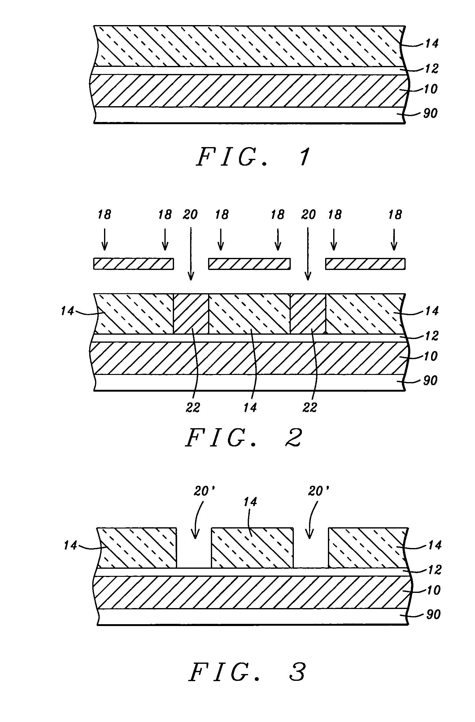
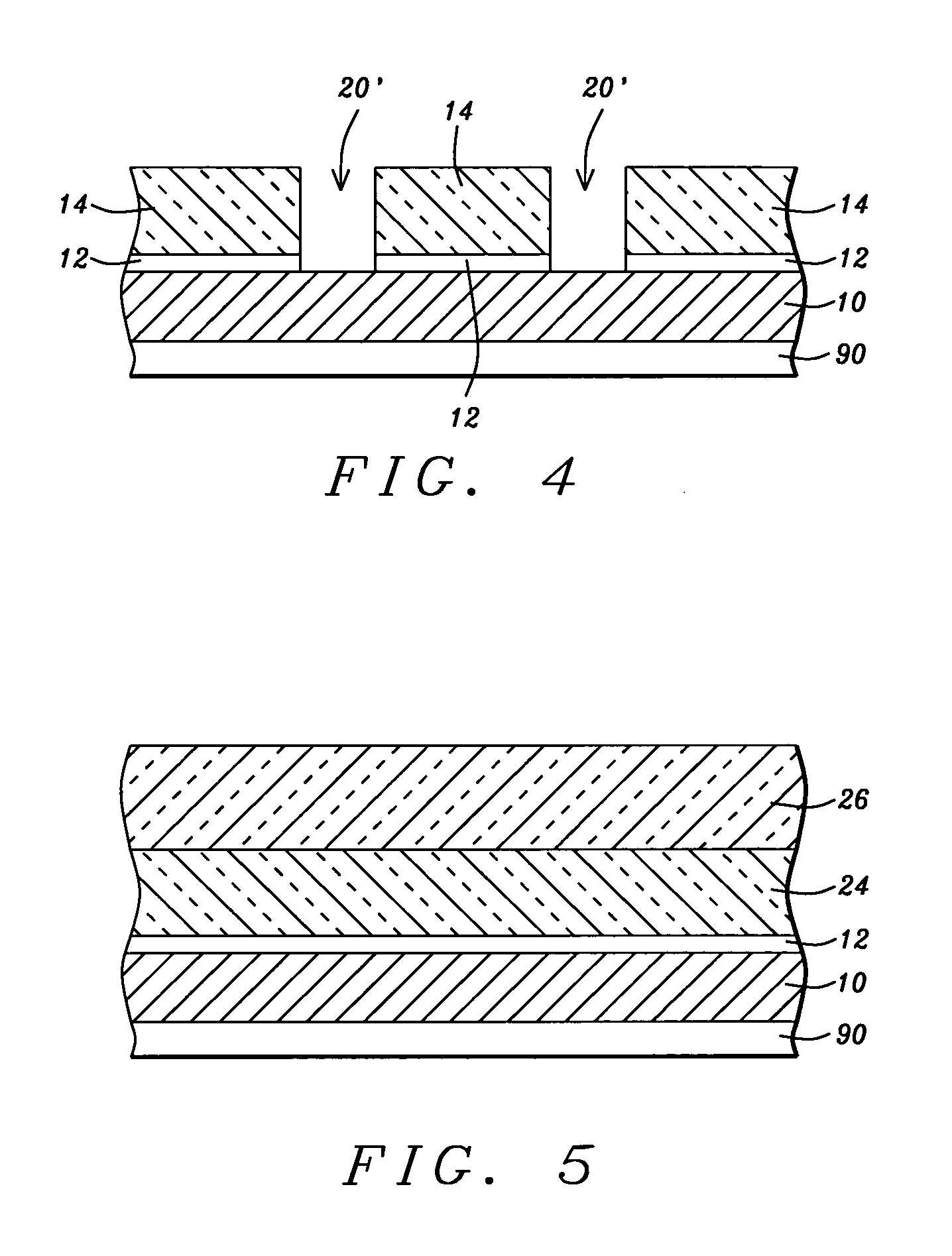
[0059] As a final step under the invention, the layer 12 of ARC is removed from the bottom surface of openings 20′, the result of which is shown in the cross section of FIG. 4. The layer 10 of metal, preferably comprising copper, is now exposed, enabling the creation of single damascene interconnects by filling openings 20′ with a conductive material, such as copper, which will be in direct contact with the layer 10 of for instance copper.

[0060] As an example of layer 12 can be cited a layer of Bottom Anti Reflective Coating (BARC), comprising either SiON or organic BARC, which can be removed from opening 20′ with a recipe comprising O2 at a flow rate between 10 and 100 sccm, N2 at a flow rate between 10 and 100 sccm, applied for a time period between about 30 and 60 seconds.

second embodiment

[0061] the invention will now be explained using FIGS. 5 through 10 for this purpose.

[0062] The cross section shown in FIG. 5 will be recognized as the cross section of FIG. 1 with the addition of a second layer 26 of PAD that has been deposited over the first layer 24 of PAD. The first layer 24 of PAD is similar to the layer 14 of PAD that has been shown in the cross section of FIG. 1.

[0063] Comments that have been made with respect to layers 10, 12 and 14 of FIG. 1 equally apply to layers 10, 12, 24 (a first layer of PAD) and 26 (a second layer of PAD) shown in cross section in FIG. 5 and are enclosed at this time by reference.

[0064] It must further be pointed out that layer 24, the first PAD layer, and layer 26, the second PAD layer, preferably comprise different types of PAD materials, as these PAD materials have previously been defined, and are exposed and subsequently developed using different types of lithographic exposures, thus allowing for the creation of openings having...

third embodiment

[0077] the invention starts with the structure that has been shown in the cross section of FIG. 2. This cross section is again shown in the cross section of FIG. 11, the exposure mask 16 and the source 18 / 20 of light energy, which are shown in FIG. 2, are omitted from the cross section shown in FIG. 11. The steps that are required to create the cross section that is shown in FIG. 1 therefore are assumed to precede the cross section shown in FIG. 11.

[0078] It must be noted in FIG. 11 that the layer 12 of ARC remains in place underneath the exposed regions 22 of the first layer 14 of PAD.

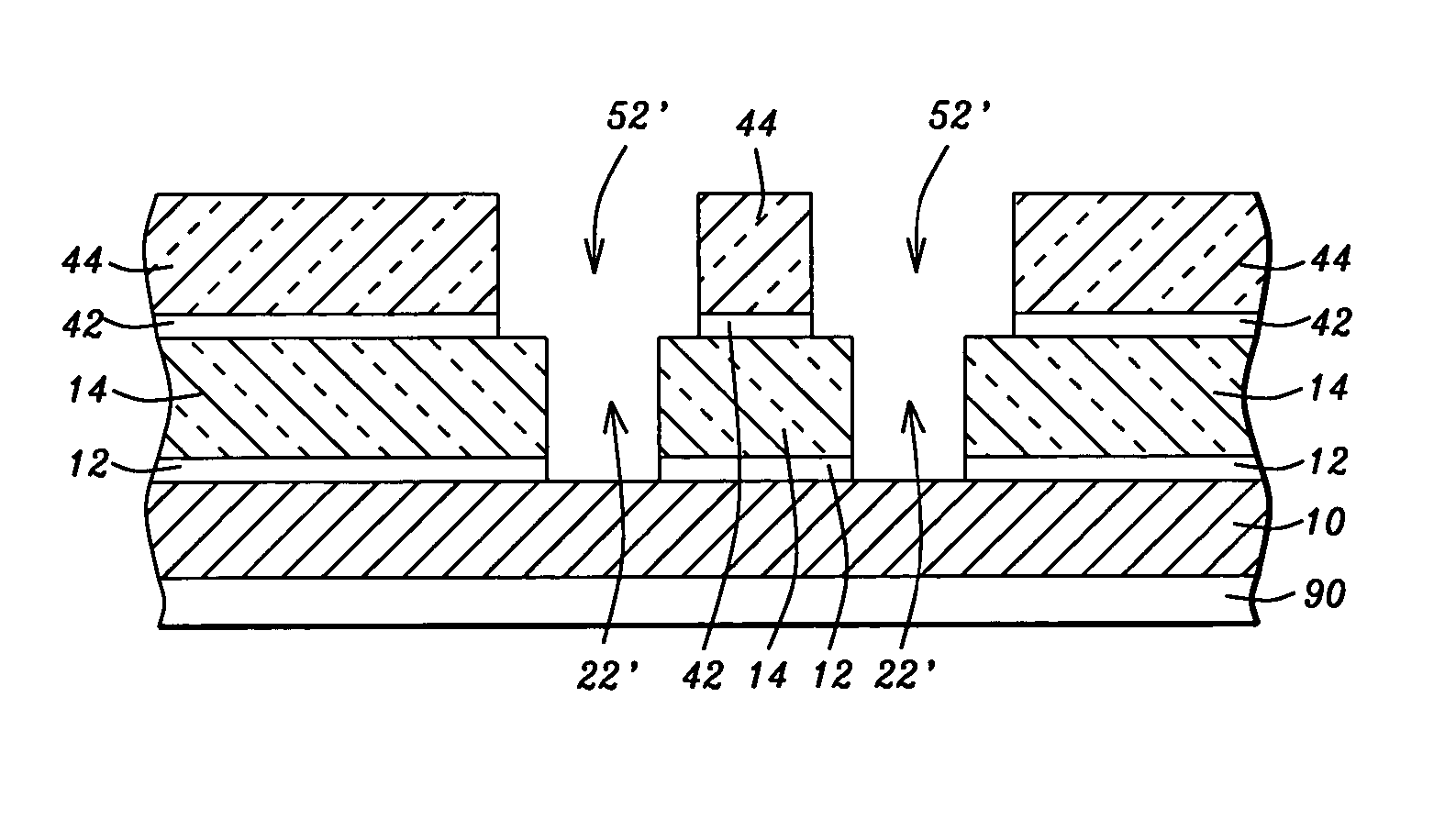
[0079]FIG. 12 shows a cross section after a second layer 42 of ARC has been deposited, for the conventional reasons as highlighted previously for the deposition of a layer of ARC, over which a second layer 44 of PAD has been deposited.

[0080] The second layer 44, as shown in the cross section of FIG. 13, is now exposed using exposure mask 46. The openings contained in exposure mask 46 are aligned wit...


PUM


Abstract

In accordance with the objectives of the invention a new method is provided for the creation of an interconnect pattern. The invention provides for a layer of Photo-Active Dielectric (PAD) to be used for the insulation material in which the interconnect pattern is created, this without the use of an overlying exposure mask of photoresist.

Description

BACKGROUND OF THE INVENTION [0001] (1) Field of the Invention [0002] The invention relates to the fabrication of integrated circuit devices, and more particularly, to a method of creating a pattern for conductive interconnects in a layer of photo-active dielectric material without using a separate layer of photoresist for the exposure and patterning of the layer of photo-active dielectric material. [0003] (2) Description of the Prior Art [0004] In the formation of semiconductor integrated circuits, it is common practice to form interconnect metal line structures on a number of different levels within the structure and interconnecting the various levels of wiring with contact or via openings. [0005] The first or lowest level of interconnect wires is typically formed as a first step in the process after which a second or overlying level of interconnect wires is deposited over the first level. [0006] The first level of interconnect wires is typically in contact with active regions in a...

Claims


Application Information

Patent Timeline
Patent Type & Authority Applications(United States)
IPC IPC(8): H01L21/4763H01L21/48H01L21/768H01L23/48H01L23/532H01L29/40
CPCH01L21/4846H01L21/76802H01L21/76807H01L21/76814H01L21/76828H01L23/5329H01L2924/0002H01L2221/1026H01L2924/09701H01L2924/00
Inventor LIU, WUPINGZHANG, BEI CHAOHSIA, LIANG CHOO
Owner CHARTERED SEMICONDUCTOR MANUFACTURING
Why Eureka
Try Eureka