Full color organic light-emtting device having color modulation layer

a technology of organic light-emitting devices and color modulation layers, which is applied in the direction of organic semiconductor devices, discharge tubes/lamp details, discharge tubes luminescnet screens, etc., can solve the problems of difficult white balance, cf previously formed may be contaminated, and the process of forming cf by photolithography has a disadvantage of requiring many processes and more time to fabricate oled, so as to reduce the time of fabrication and maintain white balance. , the effect o

Inactive Publication Date: 2005-05-05
SAMSUNG MOBILE DISPLAY CO LTD
View PDF20 Cites 88 Cited by
  • Summary
  • Abstract
  • Description
  • Claims
  • Application Information

AI Technical Summary

Benefits of technology

[0008] An exemplary embodiment of the present invention provides an OLED having a reduced fabrication time and a high resolution, as well as maintaining white balance even after it is driven for a long time. In an embodiment of the present invention, the OLED comprises a substrate having a red pixel region, a green pixel region, a blue pixel region and a white pixel region. First electrodes are positioned on the red, green, blue and white pixel regions of the substrate, respectively. A second electrode is positioned on the first electrodes, wherein at least one of the first electrode and the second electrode is a transparent electrode. An organic functional layer is interposed between the first and the second electrodes, where the organic functional layer has an emission layer emitting white color light. Color modulation layers for red, green and blue colors formed by a laser-induced thermal imaging (hereinafter, referred to as LITI) method are positioned on a surfaces opposite to a surfaces adjacent to the emission layer of the transparent electrodes of the red, green and blue pixel regions, respectively. Wherein the each color modulation layer has at least one of a CF and a CCM.

Problems solved by technology

But in this method, the emission layers have different lifetime characteristics one from another, so that it is difficult to maintain white balance when they are driven for a long time.
In these processes, a CF previously formed may be contaminated by a CF material of another color which is spin coated on the CF.
Thus, forming the CF by the photolithography process has a disadvantage of requiring many processes and more time to fabricate the OLED.
This makes it hard to implement a high resolution due to difficulties aligning between the metal mask with the substrate.
A further disadvantage is that the layers corresponding to the R, G and B are deposited in a separate chamber, respectively, significantly increasing an equipment investment.

Method used


Image

  • Full color organic light-emtting device having color modulation layer
  • Full color organic light-emtting device having color modulation layer
  • Full color organic light-emtting device having color modulation layer

Examples


experimental example

[EXPERIMENTAL EXAMPLE]

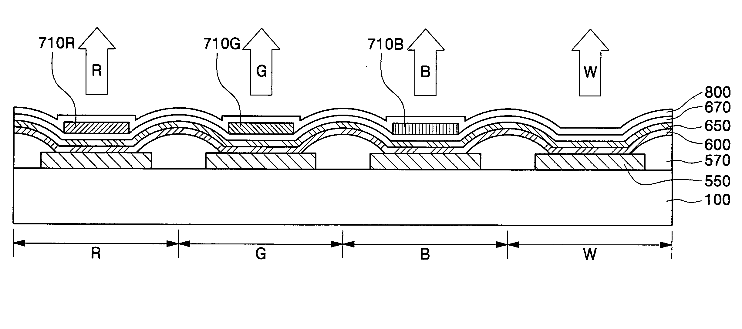
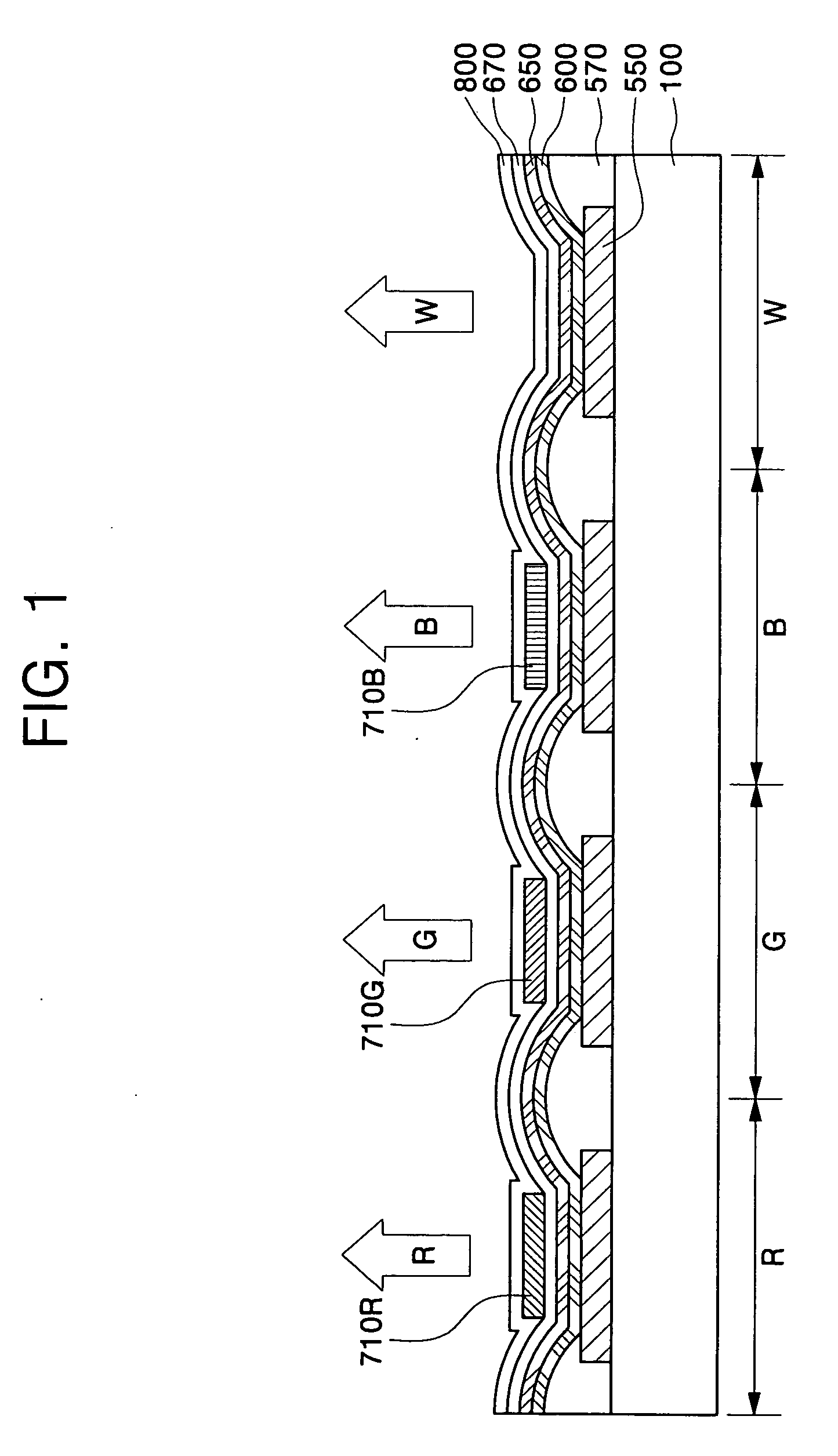
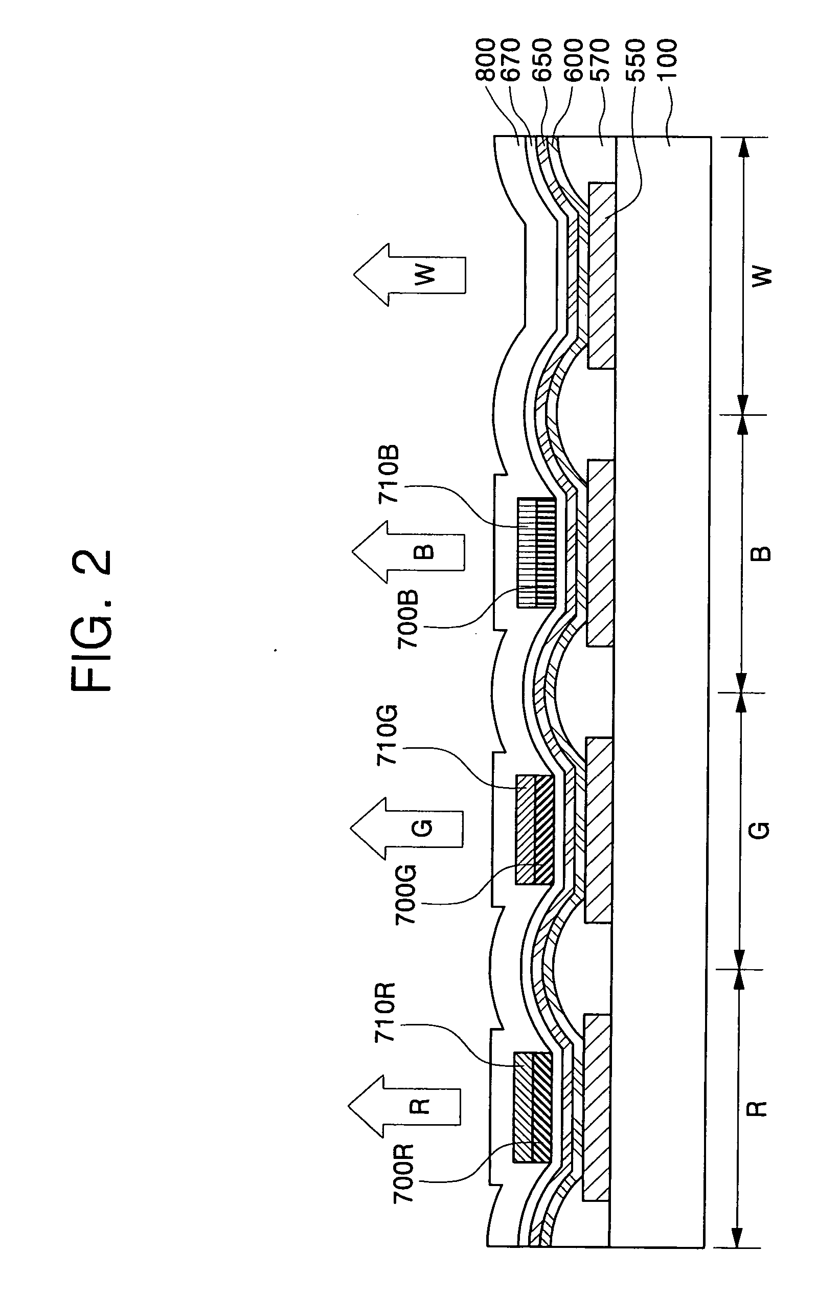
[0092] Material for the CF (manufactured by 3M Co.) was deposited on a donor film (manufactured by 3M Co.) to form a transfer layer, while preparing a substrate. The donor film was arranged to make the transfer layer face the substrate and was irradiated by an Nd-YAG laser, so that the transfer layer was transferred onto the substrate. In the transfer process, the laser power was 10 W, and the scanning speed of the laser was 7 m / sec. This process was repeated for each of red, green and blue colors, so that patterns for the red, green and blue CFs were formed on the substrate. Anode patterns were then formed on the CF patterns, respectively, and an emission layer emitting white color light was formed on the anodes. Cathodes were then formed on the emission layer, so that a full color OLED was fabricated.


PUM


Abstract

An organic light-emitting device has a color modulation layer. The organic light-emitting device comprises a substrate having a red pixel region, a green pixel region, a blue pixel region and a white pixel region. First electrodes are positioned on the red, green, blue and white pixel regions of the substrate, respectively. A second electrode is positioned on the first electrode, wherein at least one of the first electrode and the second electrode is a transparent electrode. An organic functional layer is interposed between the first and the second electrodes, where the organic functional layer has an emission layer emitting white color light. Color modulation layers for red, green and blue colors formed by a laser-induced thermal imaging (hereinafter, referred to as LITI) method are positioned on a surfaces opposite to a surfaces adjacent to the emission layer of the transparent electrodes of the red, green and blue pixel regions, respectively. Wherein the each color modulation layer has at least one of a CF and a CCM.

Description

CROSS-REFERENCE TO RELATED APPLICATION [0001] This application claims priority from U.S. patent application Ser. No. 10 / 914,119 filed on Aug. 10, 2004, which claims the benefit of Korea Patent Application No. 2003-65683, filed on Sep. 22, 2003, the disclosures of which are both hereby incorporated by reference in their entirety.1. FIELD OF THE INVENTION [0002] The present invention relates to an organic light-emitting device (OLED) and, more particularly, to an organic light-emitting device having color modulation layer. 2. BACKGROUND OF THE INVENTION [0003] In general, an organic light-emitting device (hereinafter, referred to as OLED) comprises a substrate, an anode positioned on the substrate, an emission layer positioned on the anode, and a cathode positioned on the emission layer. In the OLED having the above structure, when a voltage is applied between the anode and the cathode, holes and electrons are injected into the emission layer, and then combined in the emission layer t...

Claims


Application Information

Patent Timeline
Patent Type & Authority Applications(United States)
IPC IPC(8): H01J1/62H05B33/00H05B33/14
CPCH01L27/3209H01L27/322H01L2251/5323H01L51/5036H01L27/3244H10K59/38H10K59/12H10K50/125H10K2102/3031
Inventor SUH, MIN-CHULCHUNG, HO-KYOONLEE, SEONG-TAEKKWON, JANG-HYUK
Owner SAMSUNG MOBILE DISPLAY CO LTD
Why Eureka
Try Eureka