Plasma display device and method for driving same

a display device and plasma technology, applied in the direction of electrodes, identification means, instruments, etc., can solve the problems of unresolved problems, large ratio of scanning period tb>2/b> to period in each sub-field ts, and improvement of light-emitting luminance, etc., to achieve shortening the scanning period, improving the image quality, and increasing the cost

Inactive Publication Date: 2005-05-05
PIONEER CORP
View PDF5 Cites 19 Cited by
  • Summary
  • Abstract
  • Description
  • Claims
  • Application Information

AI Technical Summary

Benefits of technology

[0031] In view of the above, it is an object of the present invention to provide a plasma display device and its driving method which are capable of displaying an excellent image, without an increase in costs caused by an increased number of driving circuits, by shortening a scanning period while writing discharge is made, with reliability, to occur and by improving contrast.

Problems solved by technology

However, in reality, since the PDP tends to be made further big-screen which, as a result, increases the number of cells (pixels), if the PDP is made high-definition in a state where configurations of the PDP and methods for driving the PDP remain conventional, it is unavoidable that a ratio of a scanning period T2 to a period in each sub-field TS becomes large.
Moreover, another problem having not yet been solved by the conventional configuration of a PDP and by the conventional driving method is contrast.
However, according to this method, since cells appear in which insufficient writing discharge occurs when time during which the scanning pulse P8 is applied is made shorter, a cell that should be lit originally is not lit, which, as a result, does not lead to improvement of light-emitting luminance.
However, this method has a problem in that, though the scanning period T2 can be reduced to a half, the number of circuits to drive each of data electrodes increases, which, as a result, causes high costs.
However, in this case, since the priming effect given by the pre-discharge decreases, if a width of a scanning pulse to be applied is the same as in the conventional case, writing discharge is not made to occur easily and a good image cannot be obtained.
However, the PDP and its driving method disclosed in Japanese Patent Application Laid-open Nos. 2002-297091 and 2002-150949 and in Japanese Patent No. 2655500 have such problems as described below.
That is, the PDP and its driving method disclosed in Japanese Patent Application Laid-open No. 2002-297091 has a problem in that application of a pulse having complicated waveform to the first and second newly-mounted auxiliary discharge electrodes is required and an increase in costs occurs which is caused by an increase in the number of driving circuits.
Next, the PDP and its driving method disclosed in the Japanese Patent Application Laid-open No. 2002-150949 has also a problem in that, though the increase in costs for driving circuits being the problem having occurred in the Japanese Patent Application Laid-open No. 2002-297091 can be avoided, if discharge cells being adjacent to each other in up and down directions are made simply to communicate with each other, sustaining discharge spreads easily in cells being adjacent to each other in a column direction via a gap among pairs of electrodes prepared to cause auxiliary discharge to occur and there is a fear of occurrence of erroneous discharge.
To solve this problem, in the PDP and its driving method disclosed in Japanese Patent Application Laid-open No. 2002-150949, the groove is formed above a longitudinal rib on the bulk-increased layer; however, since the groove is mounted in a remote place, the priming effect has to ripple through such the far-located groove and, due to rippling in the far distance, the priming effect cannot be exerted sufficiently.
Moreover, the PDP disclosed in the Japanese Patent Application Laid-open No. 2002-1500949 has also such a problem as described below.
As a result, when a scanning pulse is applied, though an intense electric field by wall charges is generated in a display cell, no superimposed electric field by wall charges exists in a clearance and, therefore, no intense electric field is generated, That is, there is a problem that discharge to exert a priming effect does not occur easily in the clearance in a scanning period.
However, since discharge occurs in a sustaining period, useless discharge occurs below a light-shielded portion every time a sustaining pulse is applied, causing an increase in power consumption.
Moreover, the above method in which a scanning period is shortened is not effective in improving contrast being the second problem to be solved.
In the PDP and its driving method disclosed in Japanese Patent No. 2655500, since a priming cell and a display portion are integrally constructed, sustaining discharge spread in a manner to turn around the priming cell and, therefore, light is intercepted by the light-shielded portion in the priming portion and the intercepted light becomes useless.
Also, since the priming discharge spreads in a manner to turn around the display portion, light emitted due to the priming discharge cannot be completely intercepted.
This means that an effect to increase contrast is not complete.
Moreover, the above method to improve contrast is not effective in shortening the scanning period being the first problem to be solved.

Method used


Image

  • Plasma display device and method for driving same
  • Plasma display device and method for driving same
  • Plasma display device and method for driving same

Examples


first embodiment

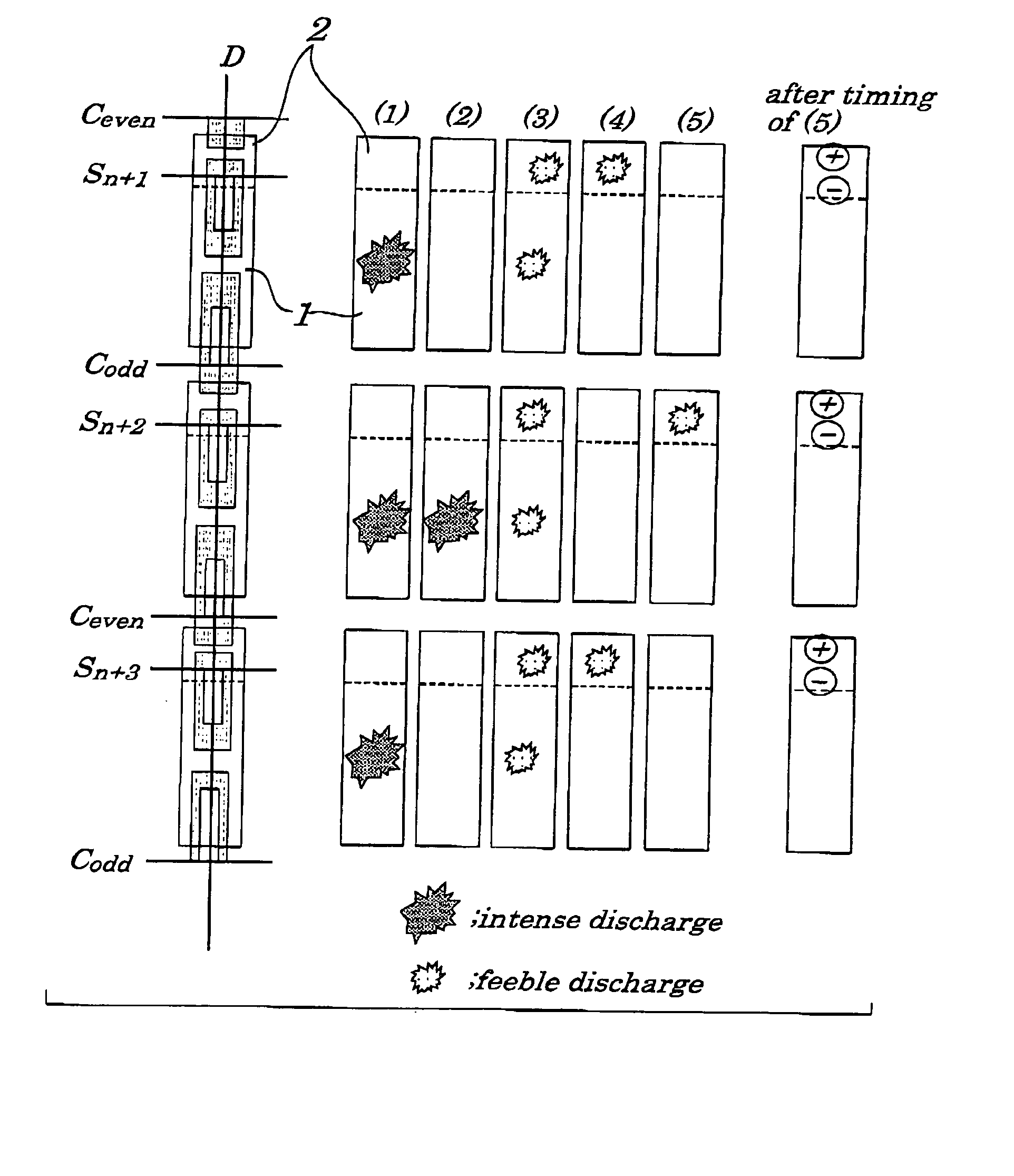
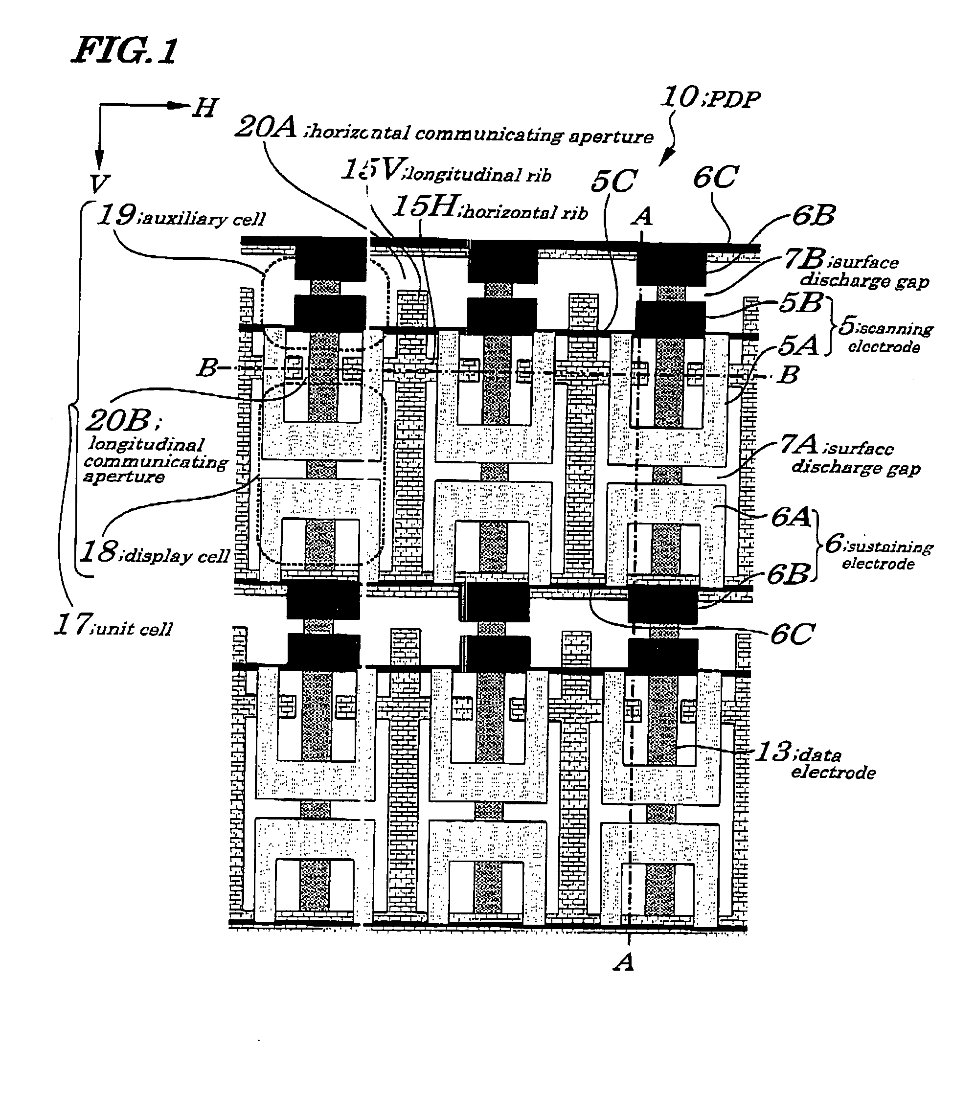
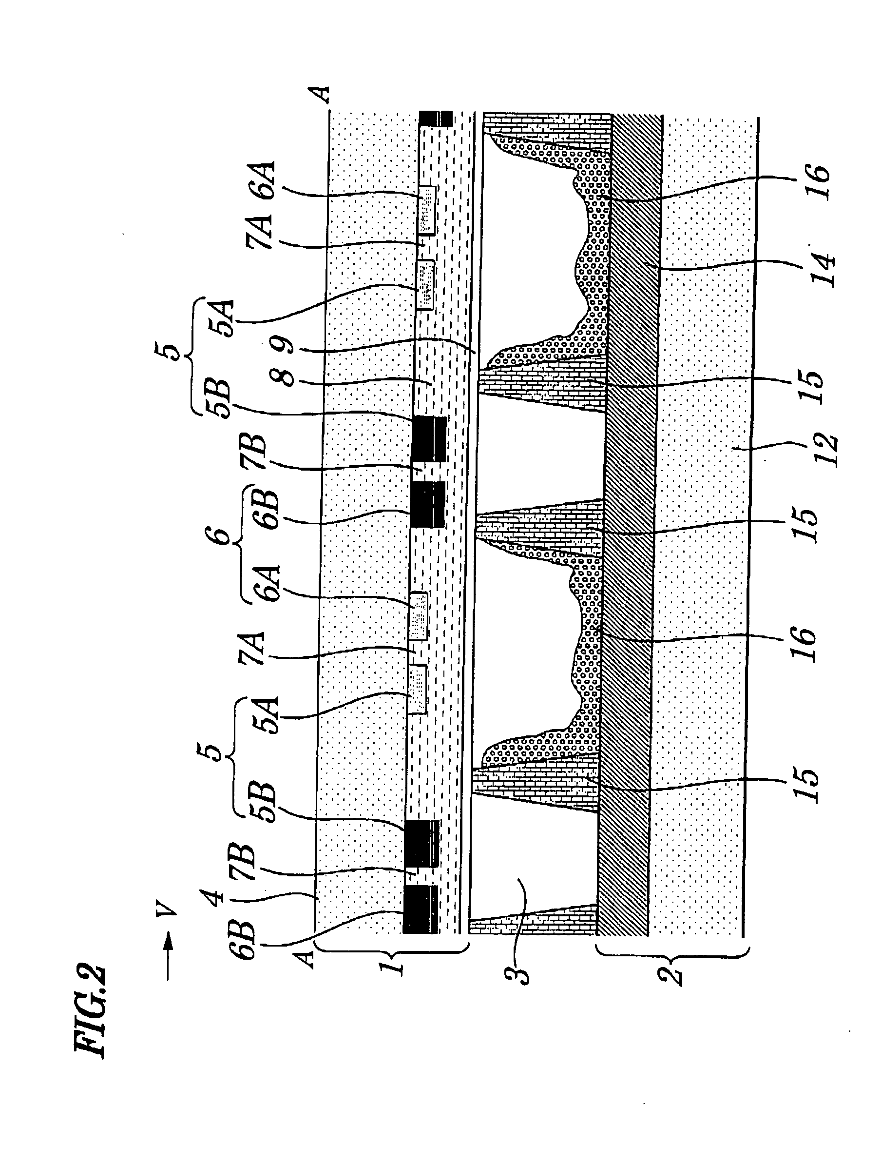
[0076]FIG. 1 is a plan view schematically showing configurations of a PDP 10 making up a main component of a plasma display device of a first embodiment of the present invention. FIG. 2 is a cross-sectional view of FIG. 1 taken along a line A-A. FIG. 3 is a cross-sectional view of FIG. 1 taken along a line B-B. FIG. 4 is a cross-sectional view showing an example of a partially modified configuration of the PDP shown in FIG. 1 taken along a line B-B. FIG. 5 is a diagram showing waveforms of a voltage applied during a pre-discharging period when the PDP 10 of FIG. 1 is driven. FIG. 6 is a diagram showing waveforms of a voltage applied during a scanning period when the PDP 10 of FIG. 1 is driven. FIG. 7 is a diagram showing waveforms of a voltage applied during a sustaining period when the PDP 10 of FIG. 1 is driven. FIG. 8 is a plan view schematically illustrating operations of the PDP 10 of FIG. 1 during the pre-discharging period when the PDP 10 is driven. FIG. 9 is a plan view sche...

second embodiment

[0092]FIG. 13 is a plan view schematically showing configurations of a PDP 21 making up a main component of a plasma display device according to a second embodiment of the present invention. Configurations of the PDP 21 of the second embodiment differ greatly from those employed in the first embodiment in that a place where a longitudinal communicating aperture is formed is changed and a shape of a transparent electrode is changed. The PDP 21 making up a main component of the plasma display device of the embodiment is so configured, as shown in FIG. 13, that a longitudinal communicating aperture 20B is formed at an end of a display cell 18 and, in the display cell 18, an L-shaped transparent electrode 5A′ making up a scanning electrode 5 and an L-shaped transparent electrode 6A′ making up a sustaining electrode 6 are arranged in a manner to face each other with a surface discharge gap 7A being interposed between the L-shaped transparent electrodes 5A′ and 6A′. Except these, the conf...

third embodiment

[0095]FIG. 14 is a plan view schematically for showing configurations of a PDP 22 making up a main component of a plasma display device according to a third embodiment of the present invention. Configurations of the PDP 22 of the third embodiment differ greatly from those employed in the first embodiment in that no horizontal communicating aperture exists and configurations of an auxiliary cell are changed. In the PDP 22 making up a main component of the plasma display device of the third embodiment, as shown in FIG. 14, such a horizontal communicating aperture 20A as employed in the first embodiment does not exist and, in an auxiliary cell 19, a belt-shaped bus base portion 5C making up a scanning electrode 5 and a belt-shaped bus base portion 6C making up a sustaining electrode 6 are arranged in a manner to face each other with a surface discharge gap 7B interposed between the belt-shaped bus base portions 5C and 6C.

[0096] By configuring as above, following effects can be obtaine...


PUM


Abstract

A plasma display device and its driving method are provided which are capable of displaying an excellent image, without an increase in costs caused by an increased number of driving circuits, by shortening a scanning period while writing discharge is made to occur with reliability and by improving contrast. In a plasma display panel (PDP) in the plasma display device, a group of unit cells is formed at intersecting points between each of groups of row electrodes and a group of column electrodes. Each of unit cells is made up of a display cell and auxiliary cell and is surrounded by a horizontal rib and a longitudinal rib. A horizontal communicating aperture is formed in the longitudinal rib to partition among two or more auxiliary cells and a longitudinal communicating aperture is formed in the horizontal rib to partition between the display cell and auxiliary cell both being arranged in the column direction.

Description

BACKGROUND 0F THE INVENTION [0001] 1. Field of the Invention [0002] The present invention relates to a plasma display device and a method for driving the plasma display device and more particularly to a three-electrode surface-discharge AC (Alternating Current)—type plasma display device including a plasma display panel (hereinafter simply called a “PDP”) as a main component. [0003] The present application claims priority of Japanese Patent Application No. 2003-370095 filed on Oct. 30, 2003, which is hereby incorporated by reference. [0004] 2. Description of the Related Art [0005] In recent years, a plasma display device having a PDP as its main component, in general, since it has many advantages in that, when compared with conventionally-used display devices such as a CRT (Cathode Ray Tube) device, an LCD (Liquid Crystal Display) device, or a like, less flicker occurs, a display contrast ratio is larger, displaying on a larger screen is made possible, it can be made thinner, it can...

Claims


Application Information

Patent Timeline
Patent Type & Authority Applications(United States)
IPC IPC(8): G09F9/313G09G3/20G09G3/288G09G3/291G09G3/293G09G3/294G09G3/298G09G3/36H01J11/12H01J11/14H01J11/22H01J11/24H01J11/26H01J11/28H01J11/34H01J11/36
CPCG09G3/288G09G3/298G09G3/2986G09G2310/0267G09G2320/0228H01J2211/444H01J11/12H01J11/24H01J11/36H01J2211/245H01J2211/365G09G2320/0238H01J11/20
Inventor FURUTANI, TAKASHIYOSHIOKA, TOSHIHIRO
Owner PIONEER CORP
Why Eureka
Try Eureka