Eureka AIR delivers breakthrough ideas for toughest innovation challenges, trusted by R&D personnel around the world.

Method for simulating the movement of particles

Active Publication Date: 2005-05-05
SYNOPSYS SWITZERLAND
View PDF2 Cites 9 Cited by
  • Summary
  • Abstract
  • Description
  • Claims
  • Application Information

AI Technical Summary

Benefits of technology

[0036] It is possible that one of the phases is amorphous and the other is crystalline. Then the method can be applied to determine dopant redistribution during SPE. This allows one to study accurately the dopant redistribution during SPE and calculate effects such as Indium dose loss (i.e. movement of Indium atoms out of the silicon), Arsenic dose loss, Fluorine dose loss, Arsenic dopant activation, Boron dose loss and Boron uphill diffusion.

Problems solved by technology

The implantation of a high dose of dopant atoms causes a lot of crystal damage to the exposed semiconductor surface.
Until now there is no process simulation available with which it is possible to determine accurately the movement and redistribution of the dopants during annealing steps in a medium having two different phases, particularly during SPE regrowth.

Method used


Image

  • Method for simulating the movement of particles
  • Method for simulating the movement of particles
  • Method for simulating the movement of particles

Examples


Embodiment Construction

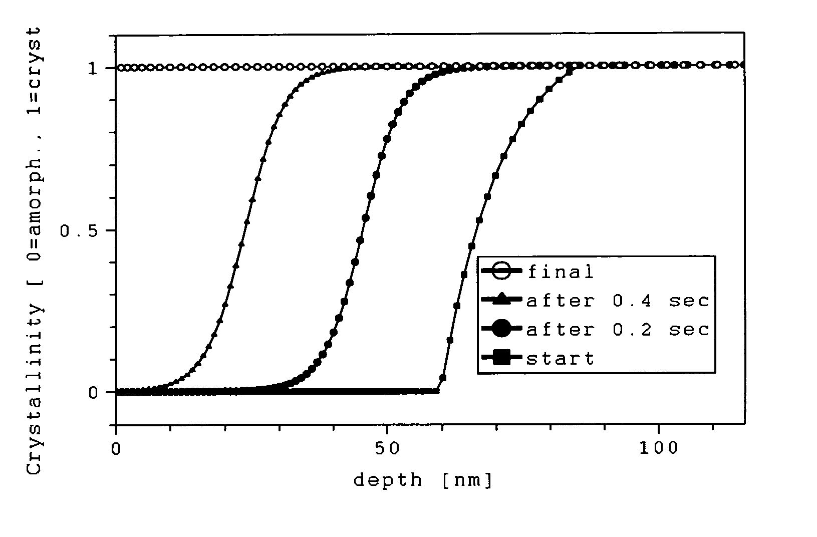
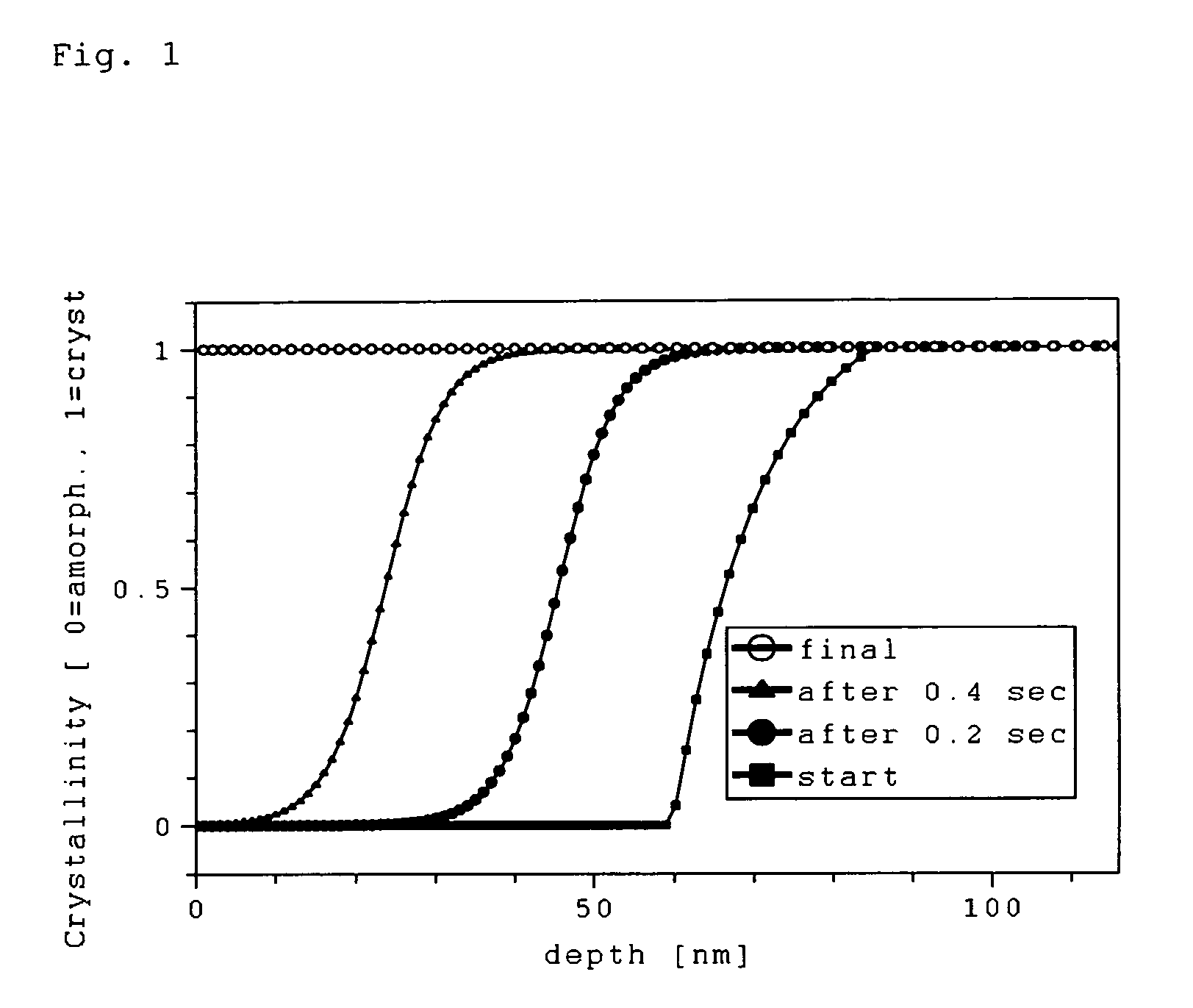
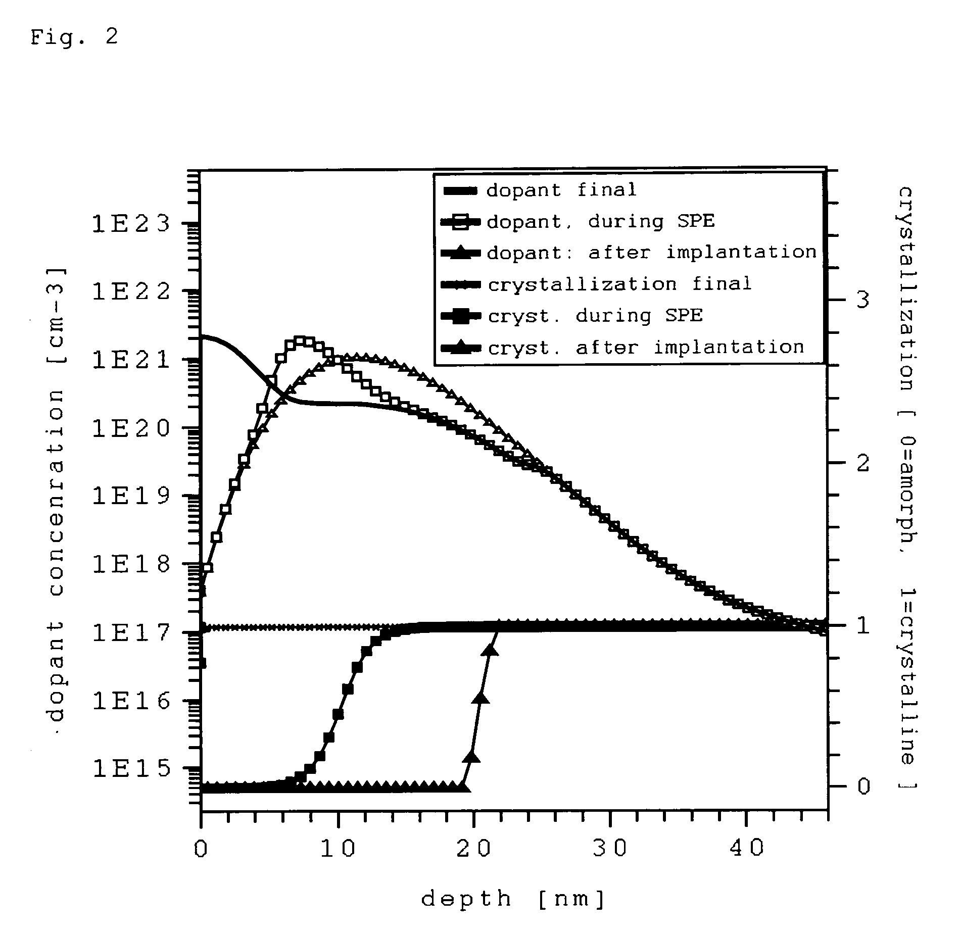
[0043] As a practical embodiment of the method, the calculation for dopant redistribution during SPE regrowth will be presented in detail. It has been implemented in the process simulator FLOOPS (FLOOPS User Manual, Release 9.0, ISE Integrated System Engineering AG, Zurich, Switzerland, 2003). In this example the high temperature annealing of a silicon wafer is considered, parts of which have been amorphized by the implantation of indium atoms at a dose of 1015 atoms per cm2 and an implantation energy of 15 keV. After the ion implantation, a temperature treatment of up to 2 minutes at 600° C. is considered, during which SPE regrowth occurs.

[0044] The following sequence of two subsequent process steps, which can be part of a fabrication process of a silicon device, is assumed: [0045] i. Ion implantation of indium atoms at a dose of 1015 atoms per cm2 and an implantation energy of 15 keV. [0046] ii. High temperature annealing of the silicon wafer, which leads to recrystallization of ...


PUM


Abstract

A method for determining the movement of particles, particularly impurities, in a medium, under the influence of a changing interface between two neighboring phases. In a first step, the temporal and / or local evolution of said interface is determined. In a second step, the movement of said particles in dependence of the temporal and / or local evolution of the phase interface as determined in the first step is calculated. Optionally, the distribution of the particles within the medium at a certain time is then determined.

Description

BACKGROUND OF THE INVENTION [0001] The invention relates to a method for simulating the movement or distribution of particles in a medium under the influence of a changing phase interface between two neighboring phases in said medium and to a computer program product comprising software code to perform said simulation. A changing interface in the context of the invention means an interface which moves at least partially in the course of time. [0002] The properties of most semiconductor devices, such as MOSFETs, are determined by the spatial arrangement of so-called dopant or (impurity) atoms, such as e.g. boron or arsenic atoms. In the absence of dopant atoms, the conductivity of the semiconductor is quite low. Regions with a high concentration of so called donor atoms (such as arsenic or phosphorus) are called n-type regions, because in such regions the concentration of negatively charged free electrons in the semiconductor is increased. Regions with a high concentration of so call...

Claims


Application Information

Patent Timeline
IPC IPC(8): G01N21/00G06F17/50
CPCG06F17/5018G06F2217/80G06F2217/16G06F2217/10G06F30/23G06F2111/08G06F2111/10G06F2119/08
Inventor ZECHNER, CHRISTOPH
Owner SYNOPSYS SWITZERLAND
Why Eureka
Eureka Blog
Learn More