Photonic band structure devices

Active Publication Date: 2005-05-05
QUANTUM NIL LTD +1
View PDF7 Cites 19 Cited by
  • Summary
  • Abstract
  • Description
  • Claims
  • Application Information

AI Technical Summary

Benefits of technology

[0041] This method provides a means of designing and producing an optical device for a particular application quickly and simply. The same method is applicable for any desired characteristics. It

Problems solved by technology

Photonic band structures can be designed so that bandgaps or band edges occur at particular wavelengths, but often these structures suffer from undesirable properties away from a particular wavelength

Method used


Image

  • Photonic band structure devices
  • Photonic band structure devices
  • Photonic band structure devices

Examples


Embodiment Construction

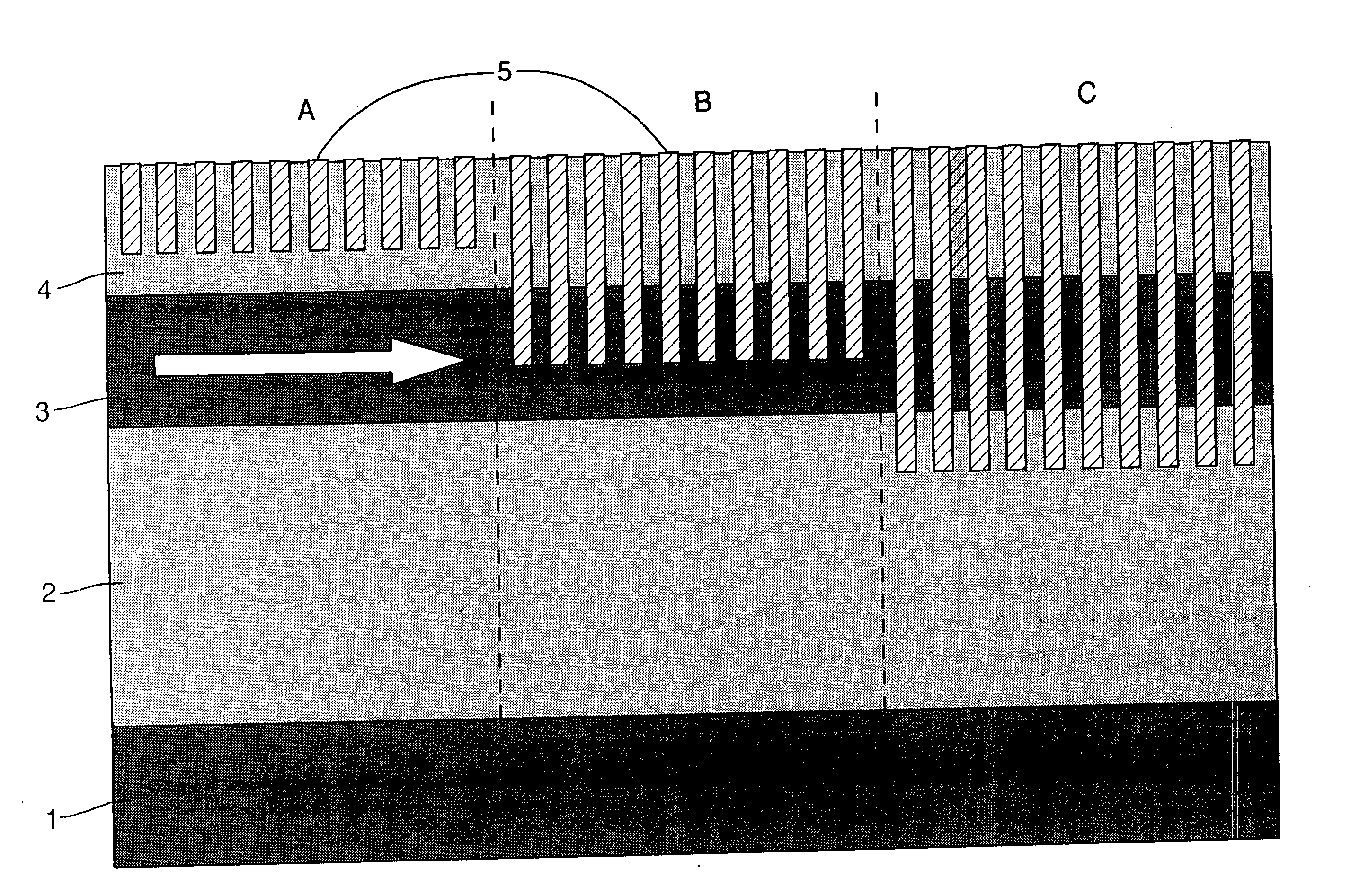
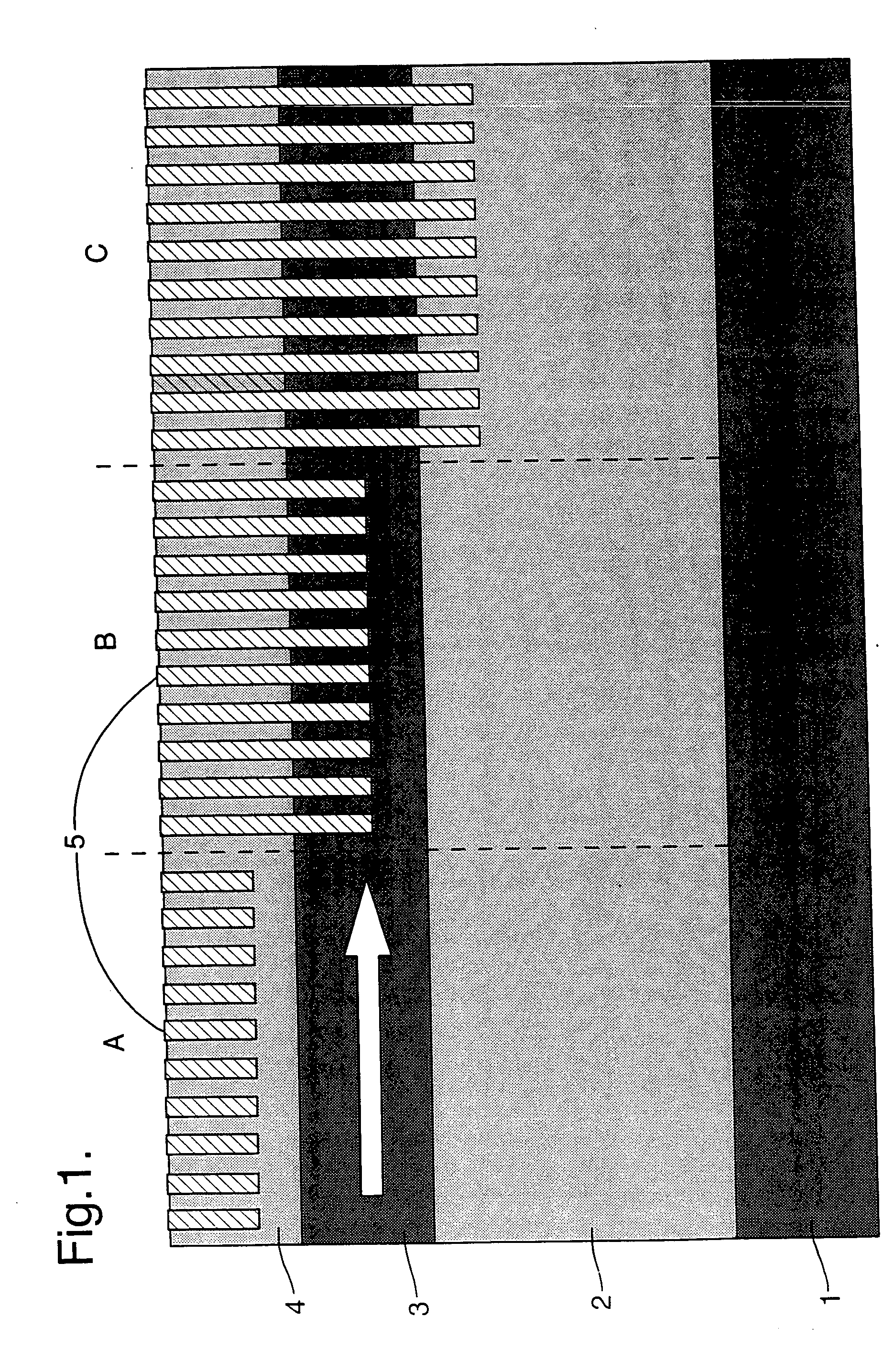
[0062] Photonic crystal structures of the type to which the present invention relates are described in WO 98 / 53351. FIG. 1 shows such a structure in cross-section.

[0063] The structure comprises a substrate 1, a buffer layer 2, a core layer 3 and a cladding layer 4. In fact FIG. 1 shows three different embodiments of these types of structure. They are two-dimensional photonic crystal structures formed in a planar waveguide. The photonic crystal is formed from an array of sub-regions 5 etched into the waveguide. As shown in FIG. 1, these sub-regions can be formed in the cladding only (section A), they can be formed in the core (section B) or they can be formed in the buffer layer (section C) or any combination of these three. This gives rise to a periodic dielectric structure which is experienced by an optical signal propagating down the waveguide. This is fully described in co-pending U.S. patent application Ser. No. 10 / 421949 filed by Mesophotonics Limited.

[0064] WO 98 / 53351 descr...


PUM


Abstract

The invention provides a photonic structure comprising a first region (3) formed from a material having a first refractive index; and an array of sub-regions (5) formed in the first region, each sub-region having a refractive index different to the first refractive index;
    • wherein the array of sub-regions (5) can be defined by a plurality of rows and columns, wherein the position of each sub-region relative to adjacent sub-regions in each row and the properties of the sub-regions across each row are defined by parameters of a first type, and the position of each row relative to adjacent rows, and the properties of the sub-regions along each column are defined by parameters of a second type; and wherein at least one parameter of a first type and at least one parameter of the second type is varied systematically and independently across the array. The present invention gives rise to structures with photonic band structures that can be tailored to a particular application. A variation in the first type of parameter has a different effect to a variation in the second type of parameter. Variation in a first type of parameter alters the diffracting properties of each row in the stack of rows. Variation in a second type of parameter affects the reflective properties of the structure. According to another aspect of the invention, a method for manufacturing photonic structures is provided including a computer optimisation process in the design stage.

Description

FIELD OF THE INVENTION [0002] The present invention relates to a photonic band structure device. In particular, the present invention relates to planar waveguide structures incorporating photonic band structures and the design of such structures. BACKGROUND TO THE INVENTION [0003] Photonic band structure devices may be incorporated in a range of different optical systems to provide optical signal processing. In particular, photonic band structures incorporated in planar waveguide structures provide a range of functions in integrated optical circuitry or in telecommunications systems. This type of photonic band structure can also be used in other applications such as biosensors and optical data storage systems. [0004] WO 98 / 53351 filed by BTG International Limited provides a detailed description for photonic band structures in planar waveguides. The photonic band structure is provided by a lattice of sub-regions embedded in a background region. Initially the sub-regions were simply h...

Claims


Application Information

Patent Timeline
IPC IPC(8): G02B6/10G02B6/12
CPCG02B6/1225B82Y20/00
Inventor PARKER, GREGCHARLTON, MARTINZOOROB, MAJDCOX, SIMON JAMES
Owner QUANTUM NIL LTD
Why Eureka
Try Eureka