MOS transistors having recesses with elevated source/drain regions and methods of fabricating such transistors

a technology of metal oxidesemiconductor and transistor, which is applied in the direction of transistors, semiconductor devices, electrical equipment, etc., can solve the problems of increased junction leakage current of the source/drain region, abnormal epitaxial layer, and difficulty in forming a uniform epitaxial layer on the defective surface, etc., to achieve the effect of increasing the concentration of impurities

Active Publication Date: 2005-05-05
SAMSUNG ELECTRONICS CO LTD
View PDF13 Cites 29 Cited by
  • Summary
  • Abstract
  • Description
  • Claims
  • Application Information

AI Technical Summary

Benefits of technology

[0012] The top surface of the metal silicide layer may be higher than the semiconductor substrate. The MOS transistor may also include a third impurity doped region in the semiconductor substrate between the first impurity doped region and the gate electrode and a fourth impurity doped region in the semiconductor substrate between the second impurity doped region and the gate electrode. A first sidewall spacer may be provided on the third impurity doped region and a second sidewall spacer may be provided on the fourth impurity doped region such that end portions of the first and second recesses are aligned respective outer walls of the first and second sidewall spacers. The first and second impurity doped regions may have a higher concentration of impurities and / or extend deeper into the semiconductor substrate than the third and fourth impurity doped regions. In certain embodiments of the present invention, the first and second recesses may have a depth of between about 50 Angstroms and about 200 Angstroms.
[0013] In further embodiments of the present invention, MOS transistors are provided that have a gate pattern on a semiconductor substrate. A first sidewall spacer is provided adjacent to a first sidewall of the gate pattern and a second sidewall spacer is provided adjacent to a second sidewall of the gate pattern. A first recessed region is included in the semiconductor substrate that is aligned with an outer wall of the first sidewall spacer and a second recessed region is included in the semiconductor substrate that is aligned with an outer wall of the second sidewall spacer. First and second epitaxial layers are provided on the first and second recessed regions, respectively. A first impurity region is provided in the semiconductor substrate under the first sidewall spacer and a second impurity region is provided in the semiconductor substrate under the second sidewall spacer. In these embodiments, the first epitaxial layer and the semiconductor substrate below the first epitaxial layer may comprise a first high concentration impurity region that extends deeper into the semiconductor substrate than the first extended impurity region and the second epitaxial layer and the semiconductor substrate below the second epitaxial layer may comprise a second high concentration impurity region that extends deeper into the semiconductor substrate than the second extended impurity region.
[0014] In these transistors, the concentration of impurities at top surfaces of the first and second high concentration impurity regions may be higher than the concentration of impurities at bottom surfaces of the first and second high concentration impurity regions. The transistor may also include metal silicide layers on the first and second epitaxial layers. The impurity concentration of the upper portions of the first and second epitaxial layers may be greater than the impurity concentration of the lower portions of the first and second epitaxial layers.
[0015] Pursuant to still further embodiments of the present invention, method of forming MOS transistors are provided. Pursuant to these methods, a gate pattern is formed on a semiconductor substrate. Impurity ions are implanted in the semiconductor substrate to form a first impurity doped region on a first side of the gate pattern and a second impurity doped region on a second side of the gate pattern. Portions of the first and second impurity doped regions are then removed to form respective first and second recesses, and an epitaxial layer is formed on the first and second impurity doped regions that at least partially fills the first and second recesses. Finally, impurity ions are implanted in the epitaxial layer to form a first high concentration impurity doped region adjacent the first side of the gate pattern and a second high concentration impurity doped region adjacent the second side of the gate pattern.
[0016] In these methods, a chemical dry etching technique may be used to form the first and second recesses and / or selective epitaxial growth techniques may be used to form the epitaxial layer. First and second sidewall spacers may also be formed on the respective first and second sidewalls of the gate pattern prior to the removal of portions of the first and second impurity doped regions. The first and second high concentration impurity doped regions may be formed such that they extend into the semiconductor substrate below the epitaxial layer. The methods may also include forming a metal silicide layer on the epitaxial layer. The top surface of the metal silicide layer may be higher than the semiconductor substrate. In these methods, the processing steps subsequent to the formation of the first and second impurity doped regions may all be carried out at a temperature of less than 700 degrees Celsius. The methods may also include cleaning the semiconductor substrate before and / or after the chemical dry etching technique.

Problems solved by technology

However, if metal silicide layers are formed on shallow source / drain junctions, the junction leakage current of the source / drain regions may be increased.
However, if crystalline defects or contaminants exist at the surface of the substrate, it may be difficult to form a uniform epitaxial layer on the defective surface.
Such an amorphous layer may lead to an abnormal epitaxial layer.
However, increasing the annealing process time and / or the annealing temperature tends to cause additional diffusion of the impurity ions in the extension regions which can lead to a short channel effect with the MOS transistor.

Method used


Image

  • MOS transistors having recesses with elevated source/drain regions and methods of fabricating such transistors
  • MOS transistors having recesses with elevated source/drain regions and methods of fabricating such transistors
  • MOS transistors having recesses with elevated source/drain regions and methods of fabricating such transistors

Examples


Embodiment Construction

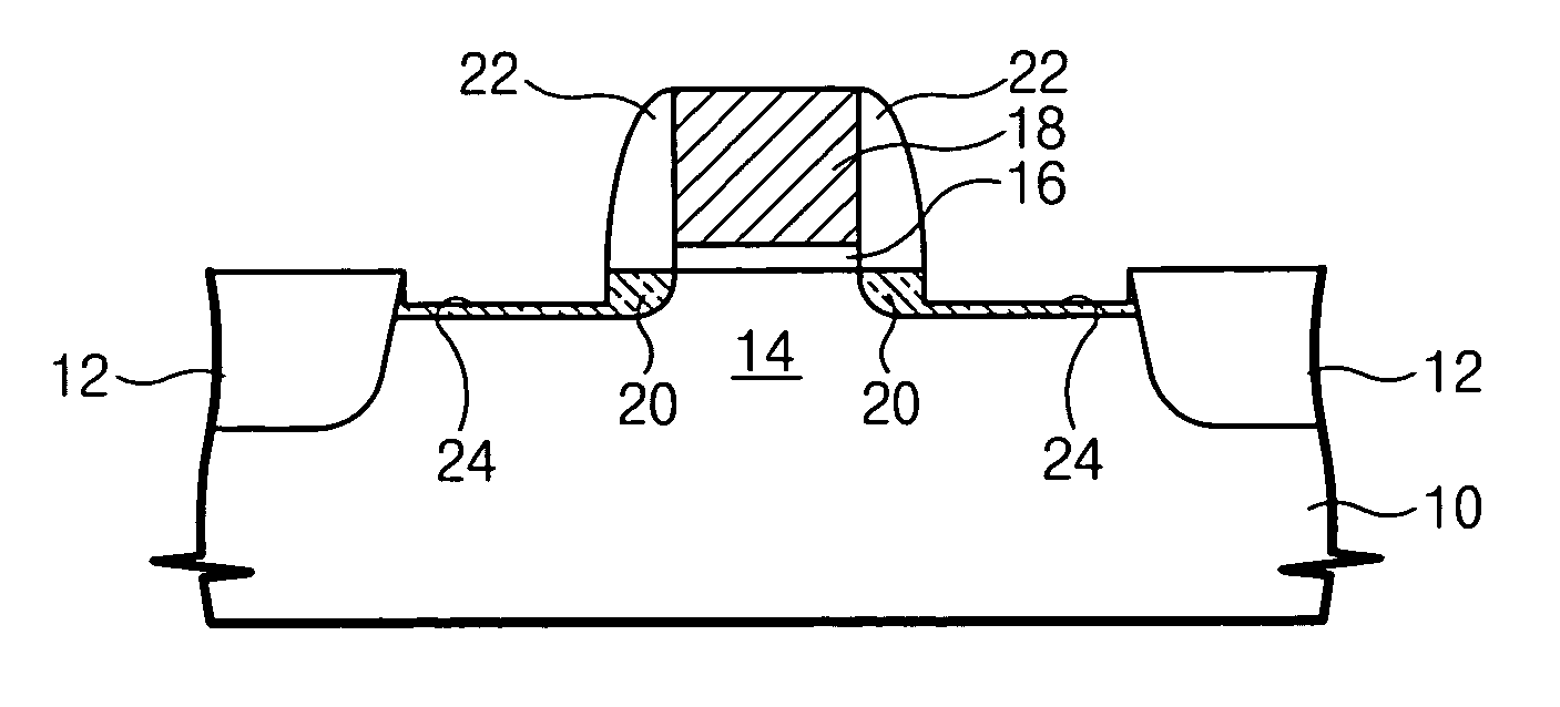
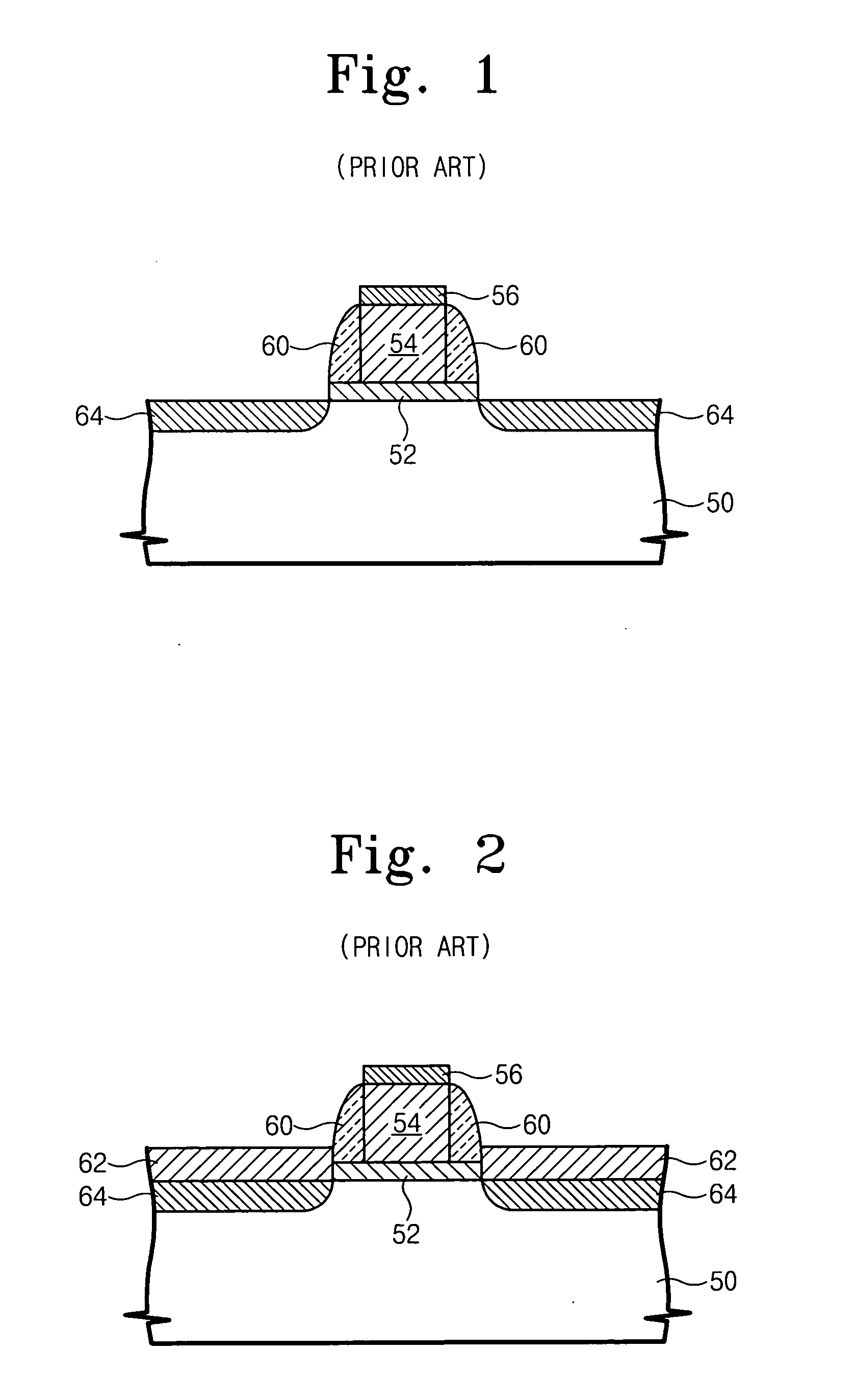
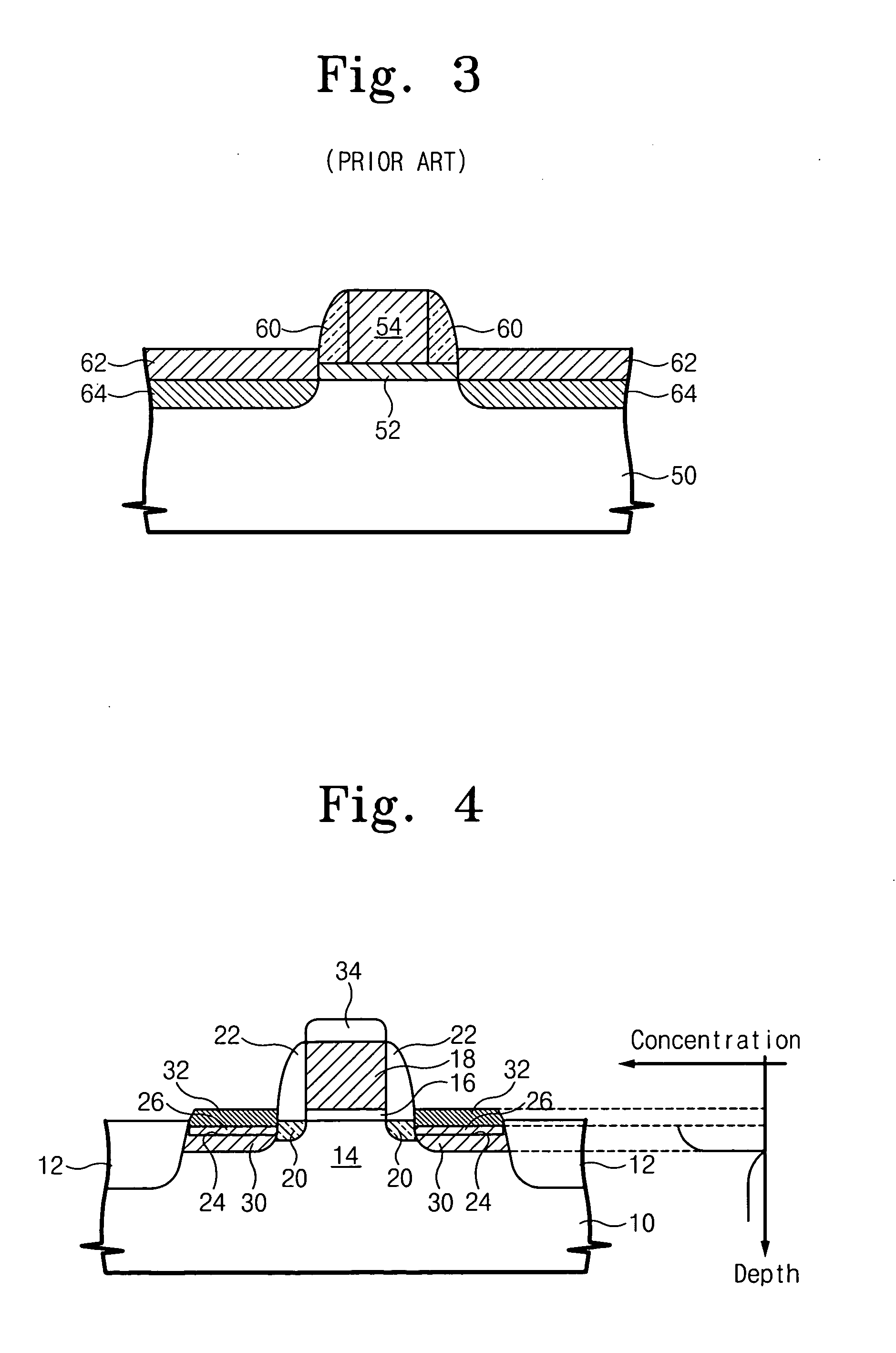
[0022] The present invention now will be described more fully hereinafter with reference to the accompanying drawings, in which embodiments of the invention are shown. This invention may, however, be embodied in many different forms and should not be construed as limited to the embodiments set forth herein. Rather, these embodiments are provided so that this disclosure will be thorough and complete, and will fully convey the scope of the invention to those skilled in the art. In the drawings, the size and relative sizes of layers and regions may be exaggerated for clarity. Like numbers refer to like elements throughout.

[0023] It will be understood that when an element such as a layer, region or substrate is referred to as being “on” another element, it can be directly on the other element or intervening elements may also be present. Similarly, when a layer or element is referred to as being “below” another layer or element, it can be directly below the other layer or element, or in...


PUM


Abstract

Metal-oxide-semiconductor (MOS) transistors having elevated source/drain regions and methods of fabricating the same are provided. The MOS transistors may include a gate pattern formed to cross over a predetermined region of a substrate. Recessed regions are provided in the substrate adjacent to the gate pattern. Epitaxial layers are provided on bottom surfaces of the recessed regions. High concentration impurity regions are provided in the epitaxial layers. The recessed regions may be formed using a chemical dry etching techniques.

Description

CROSS-REFERENCE TO RELATED APPLICATION [0001] This application claims priority under 35 U.S.C. § 119 from Korean Patent Application No. 2003-45787, filed Jul. 7, 2003, the disclosure of which is incorporated herein by reference in its entirety. FIELD OF THE INVENTION [0002] The present invention relates to semiconductor devices and, more particularly, to metal-oxide-semiconductor (MOS) transistors and methods of fabricating such transistors. BACKGROUND OF THE INVENTION [0003] As semiconductor devices having metal-oxide-semiconductor (MOS) transistors become more highly integrated, the contact sizes and junction depths of the source / drain regions of these devices have been reduced. Accordingly, a salicide (self-aligned silicide) technique is widely used in the fabrication of highly integrated MOS transistor semiconductor devices in order to allow improvement in certain electrical characteristics of the MOS transistors such as the contact resistance of the source / drain regions. Howeve...

Claims


Application Information

Patent Timeline
Patent Type & Authority Applications(United States)
IPC IPC(8): H01L21/336H01L21/425H01L21/8242H01L29/78
CPCH01L29/665H01L29/7833H01L29/66636H01L29/6659H01L21/18
Inventor SON, YONG-HOONCHOI, SI-YOUNGLEE, BYEONG-CHANLEE, DEOK-HYUNGJUNG, IN-SOO
Owner SAMSUNG ELECTRONICS CO LTD
Why Eureka
Try Eureka