Method for controlling power change for a semiconductor module

a technology of semiconductor modules and power changes, applied in the direction of semiconductor/solid-state device details, liquid/fluent solid measurements, instruments, etc., can solve the problems of relative movement, no one has adequately addressed the preservation of thermal solutions within semiconductor modules, and no previous attempts to control the rate of movement of thermal solutions, etc., to achieve the effect of preserving the reliability of materials

Active Publication Date: 2005-05-05
GLOBALFOUNDRIES US INC
View PDF18 Cites 0 Cited by
  • Summary
  • Abstract
  • Description
  • Claims
  • Application Information

AI Technical Summary

Benefits of technology

[0007] In general, the present invention provides a method for controlling power change for a semiconductor module. Specifically, under the present invention power is applied to, or removed from a semiconductor module between a full power state and a lower power state such as a zero power, nap or sleep state over a predetermined time period. This allows the rate of movement and strain rate of the thermal interface material within the semiconductor module to be controlled, thus preserving the reliability of the material. Typically, the power is changed over time between the lower power state and the full power state in a linear fashion or incrementally (e.g., in a series of steps approximating a linear slope).
[0008] A first aspect of the present invention provides a method for controlling power change for a semiconductor module, comprising: providing a thermal interface material in the semiconductor module; providing a full power state for the semiconductor module; and changing power for the semiconductor module between a lower power state and the full power state over a predetermined time period to reduce a strain rate of the thermal interface material.
[0009] A second aspect of the present invention provides a method for applying power to or draining power from a semiconductor module, comprising: providing a thermal interface material in the semiconductor module; providing a full power state for the semiconductor module; and applying power to the semiconductor module from a lower power state to the full power state or removing power from the semiconductor module from the full power state to the lower power state over a predetermined time period to reduce a strain rate of the thermal interface material.
[0010] A third aspect of the present invention provides a semiconductor module comprising a thermal interface material, wherein power is changed for the semiconductor module between a lower power state and the full power state over a predetermined time period to reduce a strain rate of the thermal interface material.

Problems solved by technology

One problem associated with this advancing technology is the ability to cool high power devices with cooling technologies that are affordable and reliable.
One of the biggest challenges for thermal solutions is surviving power cycling such as during powering on or off, or while entering and exiting sleep mode.
This causes relative movement when there are significant thermal excursions.
Heretofore, no one has adequately addressed the preservation of a thermal solution within a semiconductor module.
Specifically, no previous attempts have been made to control the rate of movement of a thermal solution during power cycling.

Method used


Image

  • Method for controlling power change for a semiconductor module
  • Method for controlling power change for a semiconductor module
  • Method for controlling power change for a semiconductor module

Examples


Embodiment Construction

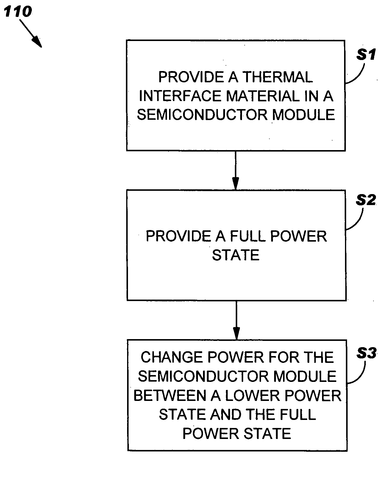
[0023] As indicated above, the present invention provides a method for controlling power change for a semiconductor module. Specifically, under the present invention power is applied to, or removed from a semiconductor module between a lower power state such as a zero power, nap or sleep state and a full power state over a predetermined time period. This allows the rate of movement and strain rate of the thermal interface material within the semiconductor module to be controlled, thus preserving the reliability of the material. Typically, the power is changed over time between the lower power state and the full power state in a linear fashion or incrementally (e.g., in a series of steps approximating a linear slope).

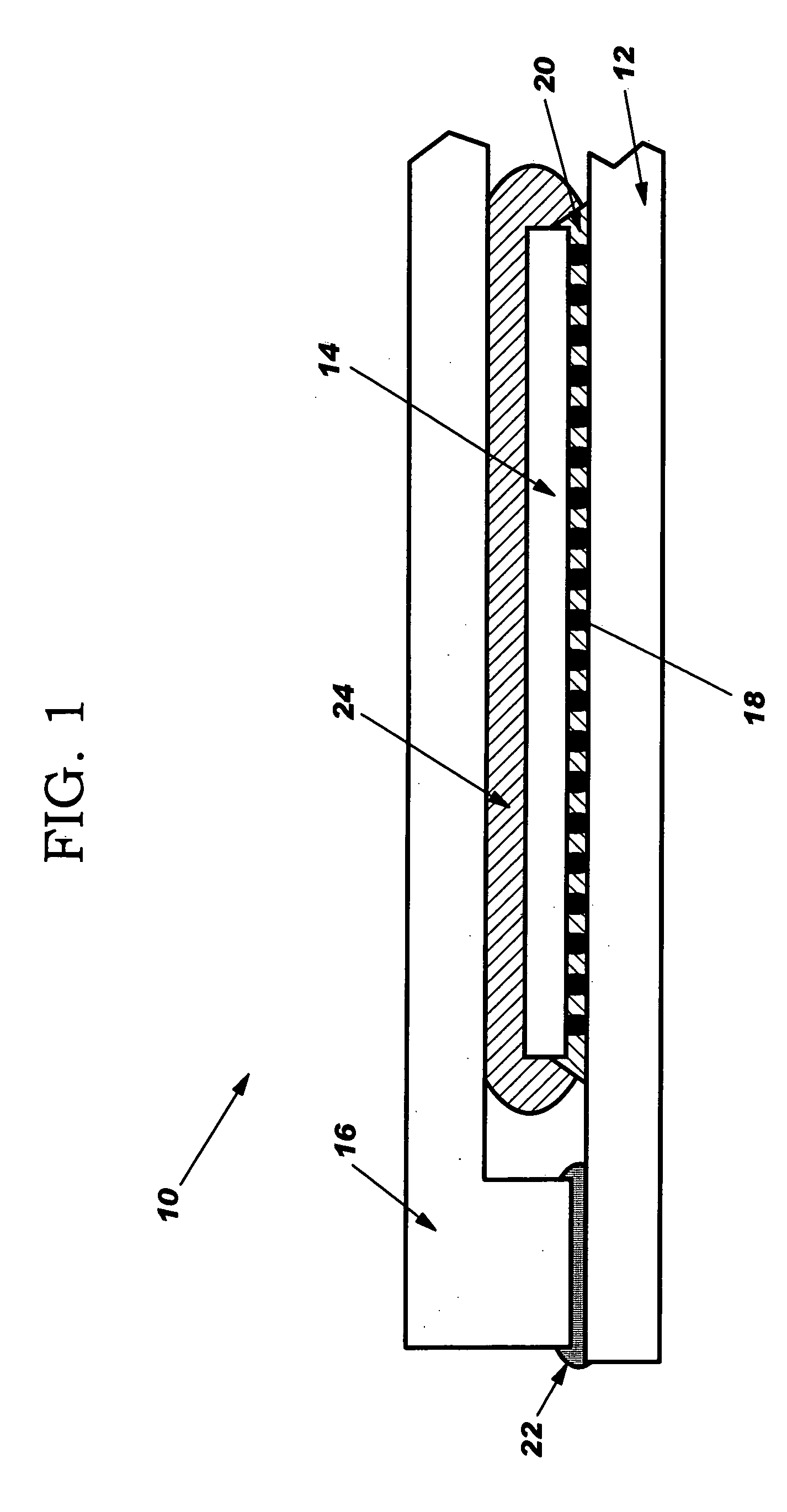
[0024] Referring now to FIG. 1, a semiconductor module 10 (hereinafter module 10) is shown. As depicted, module 10 includes chip carrier 12, chip 14 and lid 16. As known in the art, chip 14 can be attached to chip carrier 12 (e.g., which could be alumina, glass ceramic,...


PUM


Abstract

The present invention provides a method for controlling power change for a semiconductor module. Specifically, under the present invention power is applied to, or removed from a semiconductor module between a lower power state such as a zero power, nap or sleep state and a full power state over a predetermined time period. This allows the rate of movement and strain rate of the thermal interface material within the semiconductor module to be controlled, thus preserving the reliability of the material. Typically, the power is changed over time between the lower power state and the full power state in a linear fashion or incrementally.

Description

BACKGROUND OF THE INVENTION [0001] 1. Field of the Invention [0002] The present invention generally relates to a method for controlling power change for a semiconductor module. Specifically the present invention provides a way to gradually apply power to or remove power from a semiconductor module so that a thermal interface therein can be preserved. [0003] 2. Related Art [0004] As electronic devices become smaller, and operating frequencies increase, chip power density is continuing to rise. One problem associated with this advancing technology is the ability to cool high power devices with cooling technologies that are affordable and reliable. One of the biggest challenges for thermal solutions is surviving power cycling such as during powering on or off, or while entering and exiting sleep mode. Most current semiconductor modules include components that expand at different rates. This causes relative movement when there are significant thermal excursions. Since many thermal solut...

Claims


Application Information

Patent Timeline
Patent Type & Authority Applications(United States)
IPC IPC(8): G06F1/20G06F1/26H01L23/42
CPCG06F1/206Y02B60/1275H01L23/42H01L2224/16H01L2224/73253H01L2924/09701H01L2924/16152G06F1/26H01L2224/73204H01L2224/32225H01L2224/16225H01L2924/00Y02D10/00
Inventor EDWARDS, DAVID L.
Owner GLOBALFOUNDRIES US INC
Why Eureka
Try Eureka