Semiconductor storage apparatus and method for controlling semiconductor storage apparatus

a technology of semiconductor storage apparatus and semiconductor storage, which is applied in the direction of memory address/allocation/relocation, instruments, computing, etc., can solve the problems of failure bits that cannot be maintained, the reliability of data stored by the semiconductor storage apparatus will degrade and not be maintained, and the number of failure bits also tends to change depending on the number of failure bits. , to achieve the effect of preventing the deterioration of the performance of the apparatus, maintaining the reliability of data, and prolonging the life of the apparatus

Active Publication Date: 2012-11-01
HITACHI LTD
View PDF4 Cites 45 Cited by
  • Summary
  • Abstract
  • Description
  • Claims
  • Application Information

AI Technical Summary

Benefits of technology

[0025]According to the present invention, it is possible to maintain the reliability of data, prevent the deterioration of the performance of the apparatus, and realize the longer lifetime of the apparatus.

Problems solved by technology

Under the above-described circumstance, if a data retaining period is long in the semiconductor storage apparatus, or if data in a specific area is read locally more than once, or if these conditions are combined, failure bits might occur beyond the ECC correction ability.
In this case, the reliability of data stored by the semiconductor storage apparatus will degrade and not be maintained.
Furthermore, the number of failure bits also tends to change depending on the degree of deterioration of a storage area; for example, the number of failure bits tends to increase in a storage area whose degree of deterioration is high as compared to a storage area whose degree of deterioration is low even if the read frequency is low and the elapsed time since storage of the data is short.

Method used


Image

  • Semiconductor storage apparatus and method for controlling semiconductor storage apparatus
  • Semiconductor storage apparatus and method for controlling semiconductor storage apparatus
  • Semiconductor storage apparatus and method for controlling semiconductor storage apparatus

Examples


embodiment 1

(1) Embodiment 1

(1-1) Configuration of Semiconductor Storage Apparatus

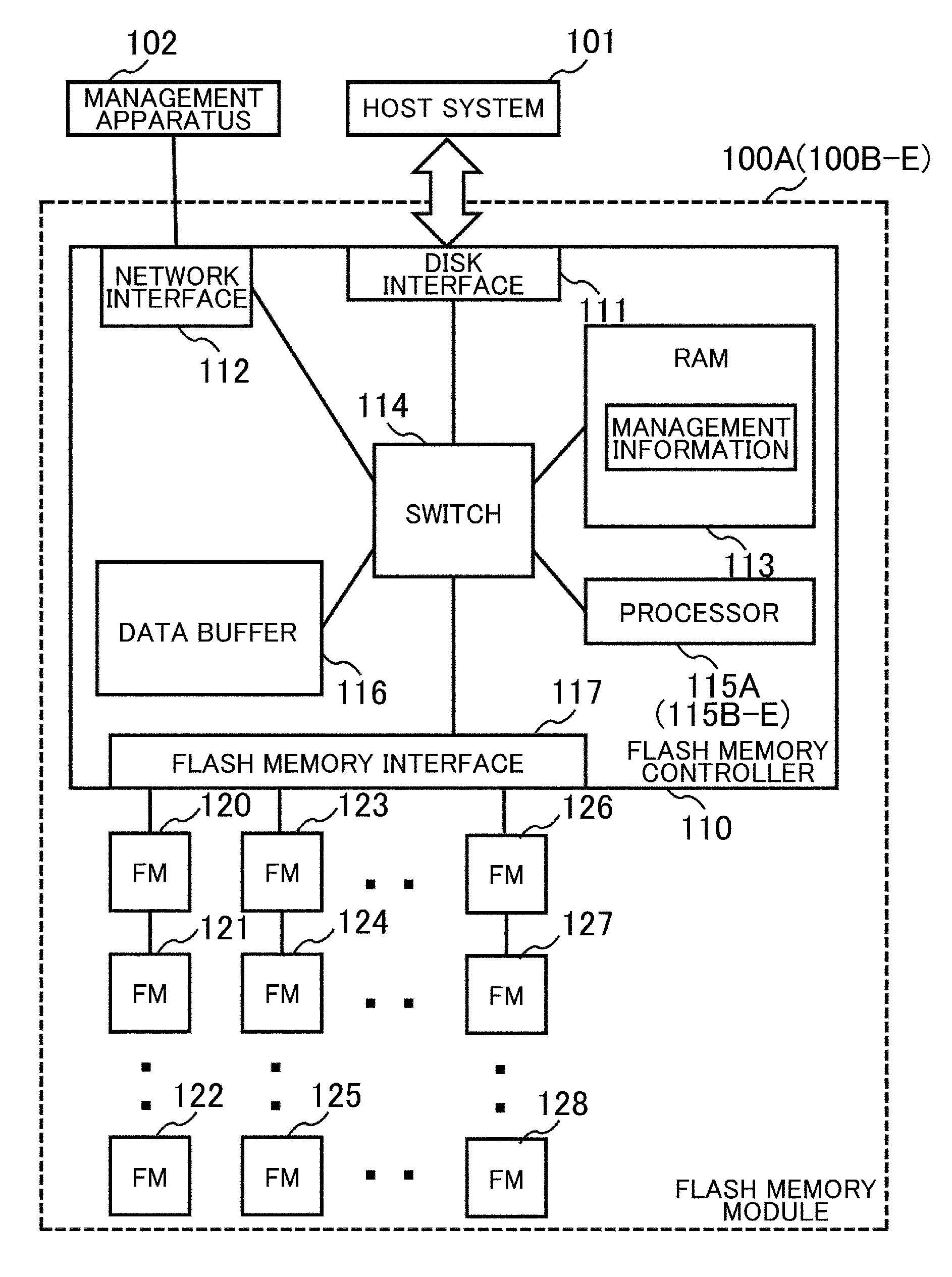
[0051]FIG. 1 shows a schematic configuration of a semiconductor storage apparatus 100A according to this embodiment as a whole. This semiconductor storage apparatus 100A is connected to a host system 101 and a management apparatus 102 so that they can communicate with each other.

[0052]The semiconductor storage apparatus 100A includes a flash memory controller 110 and a plurality of flash memories 120 to 128 (e.g. 32 units), and the flash memory controller 110 includes a disk interface 111, a network interface 112, a RAM (Random Access Memory) 113, a switch 114, a processor 115A, a data buffer 116, and a flash memory interface 117.

[0053]The disk interface 111 is connected to a storage apparatus or the host system 101 such as a server and is connected to the respective units in the flash memory controller 110 via the switch 114. The disk interface 111 receives read / write requests, LBAs (Logical Block Addresses) spec...

embodiment 2

(2) Embodiment 2

(2-1) Configuration of Semiconductor Storage Apparatus

[0128]Referring to FIG. 1, the reference numeral 100B represents a semiconductor storage apparatus 100B according to Embodiment 2 as a whole. This semiconductor storage apparatus 100B is configured in the same manner as the semiconductor storage apparatus 100A according to Embodiment 1, except that the validity of the reliability maintained period is checked. More specifically, in Embodiment 2, the number of failure bits of all pages in a block is actually read and measured, and the validity of the reliability maintained period based on the measurement result is checked. This detailed measurement of failure bits for the block will be hereinafter referred to as verification. By performing verification for each block during the reliability maintained period, a block which is different from the predicted tendency of the number of failure bits to increase can be detected, and refresh can be executed before an ECC corr...

embodiment 3

(3) Embodiment 3

(3-1) Configuration of Semiconductor Storage Apparatus

[0201]Referring to FIG. 1, the reference numeral 100C represents a semiconductor storage apparatus 100C according to Embodiment 3 as a whole. This semiconductor storage apparatus 100C is configured in the same manner as the semiconductor storage apparatus 100A according to Embodiment 1, except that deterioration of response performance to the host system 101 is prevented by preventing the concentrated execution of refresh at a specific timing and that the reliability of data stored in the semiconductor storage apparatus 100C is maintained temporally constant.

[0202]In Embodiment 1 described earlier, the refresh target block requiring the execution of refresh is obtained from the refresh management information 700 and refresh is executed on the obtained refresh target block within the reliability maintained period. However, if refresh is performed by this method, there may be a case where refresh is executed in a ma...


PUM


Abstract

A reliability maintained period is calculated for each storage area based on the degree of deterioration and read frequency for each storage area of a flash memory, and refresh is executed on each storage area in a planned manner based on the calculated reliability maintained period.
A semiconductor storage apparatus 100A is configured so that flash memories 120 to 128 and a memory controller 110 are connected and the flash memories 120 to 128 include a plurality of blocks as storage areas; and the memory controller 110 manages the degree of deterioration and read frequency of the blocks for each of the plurality of blocks, obtains a reliability maintained period of data stored in the block based on the managed degree of deterioration and read frequency of the block, and executes refresh for correcting failure bits of the relevant data by newly storing the data stored in the block in another block based on the obtained reliability maintained period.

Description

TECHNICAL FIELD[0001]The present invention relates to a semiconductor storage apparatus and a method for controlling the semiconductor storage apparatus and is specifically suited for use in a semiconductor storage apparatus, whose storage media is a flash memory, a type of electrically rewritable non-volatile memory, and a method for controlling such a semiconductor storage apparatus.BACKGROUND ART[0002]A flash memory has the property (retention property) that data stored in the flash memory gradually changes according to elapsed time since storage of the data; and also has the property (read disturb property) that as data is read more than once, the read data gradually changes. Therefore, the semiconductor storage apparatus equipped with a flash memory as storage media generally adds an ECC (Error Correcting Code), has the ability to correct a plurality of bits, to data when writing the data, and stores it in the storage area of the flash memory. Consequently, failure bits which c...

Claims


Application Information

Patent Timeline
Patent Type & Authority Applications(United States)
IPC IPC(8): G06F12/02
CPCG11C16/3404G11C16/3495G11C16/3418G06F12/0246G06F2212/72
Inventor SUZUKI, AKIFUMITSUNEHIRO, TAKASHI
Owner HITACHI LTD
Why Eureka
Try Eureka