Apparatus and methods for cooling semiconductor integrated circuit package structures

a technology of integrated circuits and semiconductors, applied in the direction of cooling/ventilation/heating modifications, semiconductor/solid-state device details, semiconductor devices, etc., can solve the problems of increasing power density, increasing system performance limitations, and increasing the problem of effective heat removal

Active Publication Date: 2008-07-01
INT BUSINESS MASCH CORP
View PDF18 Cites 48 Cited by
  • Summary
  • Abstract
  • Description
  • Claims
  • Application Information

AI Technical Summary

Benefits of technology

[0008]Exemplary embodiments described herein generally include apparatus and methods for cooling semiconductor integrated circuit (IC) chip package structures, such as MCM (multi-chip modules). More specifically, exemplary embodiments of the invention include apparatus and methods for thermally coupling the non-active (back) surface of semiconductor chips to a heat conducting device (e.g., copper thermal hat or lid) using a compliant thermally conductive material (e.g., thermal paste), wherein a thermal interface is designed to maintain the reliability of the thermally conductive compliant material by preventing / inhibiting the formation of voids in the compliant thermally conductive material as a result of power / thermal cycling which occurs under normal operation conditions of the chip package.
[0009]In particular, in one exemplary embodiment, an chip package apparatus includes an IC chip having a non-active surface, a heat conducting device having a thermal contact surface, wherein the thermal contact surface comprises one or more channels formed therein, and a TIM (thermal interface material) layer formed between, and thermally coupling, the non-active surface of the IC chip and the thermal contact surface of the heat conducting device, the TIM layer comprising a compliant thermally conductive material, wherein the one or more channels formed in the thermal contact surface are not filled with complaint thermally conductive material. The non-filled channels enable increased retention of the TIM material between the chips and the heat conducting device (e.g., thermal hat or package covers) and prevent the formation of voids in the TIM material due to thermally / mechanically induced gap changes between the chips and thermal contact surface of the heat conducting device.
[0011]In other exemplary embodiments of the invention, channels are formed in thermal contact surface regions of a heat conducting device such that when the chips are aligned to corresponding thermal contact surface regions, the channels do not overlap areas of higher than average power density (hot spot regions) on the chips, thereby minimizing any increase of the temperature of the chip “hot spots”.

Problems solved by technology

Effective heat removal becomes increasingly problematic as chip geometries are scaled down and operating speeds are increased, which results in increased power density.
Although improved IC chip module designs are being developed to operate at higher clock frequencies, increased system performance is limited primarily by the ability to implement effective heat removal mechanisms to cool the IC chip modules.
Moreover, effective cooling techniques are even more problematic for, e.g., a multi-chip module (MCM), wherein an array of chips mounted on a common substrate are thermally coupled to a common thermal hat or package lid, for example, using a compliant thermally conductive material.
Indeed, differences in thermal expansion between the materials that form the package substrate, the chips, and the thermal hat, for example, can result in both vertical and horizontal deflections during power or temperature cycling.
These deflections can lead to the migration of the compliant thermally conductive material out of the gap between the IC chips and the thermal hat, resulting in voids that increase the thermal resistance between the IC chip and the thermal hat and causing local increases in the operating temperature of the IC chips.
As noted above, such voids can cause a significant increase in the chip operating temperatures in the regions of the chip in contact with the voids.
Furthermore, difficulties arise for efficient heat removal with respect to IC chips, such as processors, that have “hot spot” regions, which can have a heat flux significantly greater than the average heat flux, resulting in temperatures significantly hotter than the average chip temperature.
A thermal solution that may be adequate for efficiently removing heat from a region of a chip having an average chip power density may not be adequate for removing heat from a “hot spot” region of the chip, i.e., a region having an above average chip power density, which can result in failure of the chip devices within or near the “hot spot” region.

Method used


Image

  • Apparatus and methods for cooling semiconductor integrated circuit package structures
  • Apparatus and methods for cooling semiconductor integrated circuit package structures
  • Apparatus and methods for cooling semiconductor integrated circuit package structures

Examples


Embodiment Construction

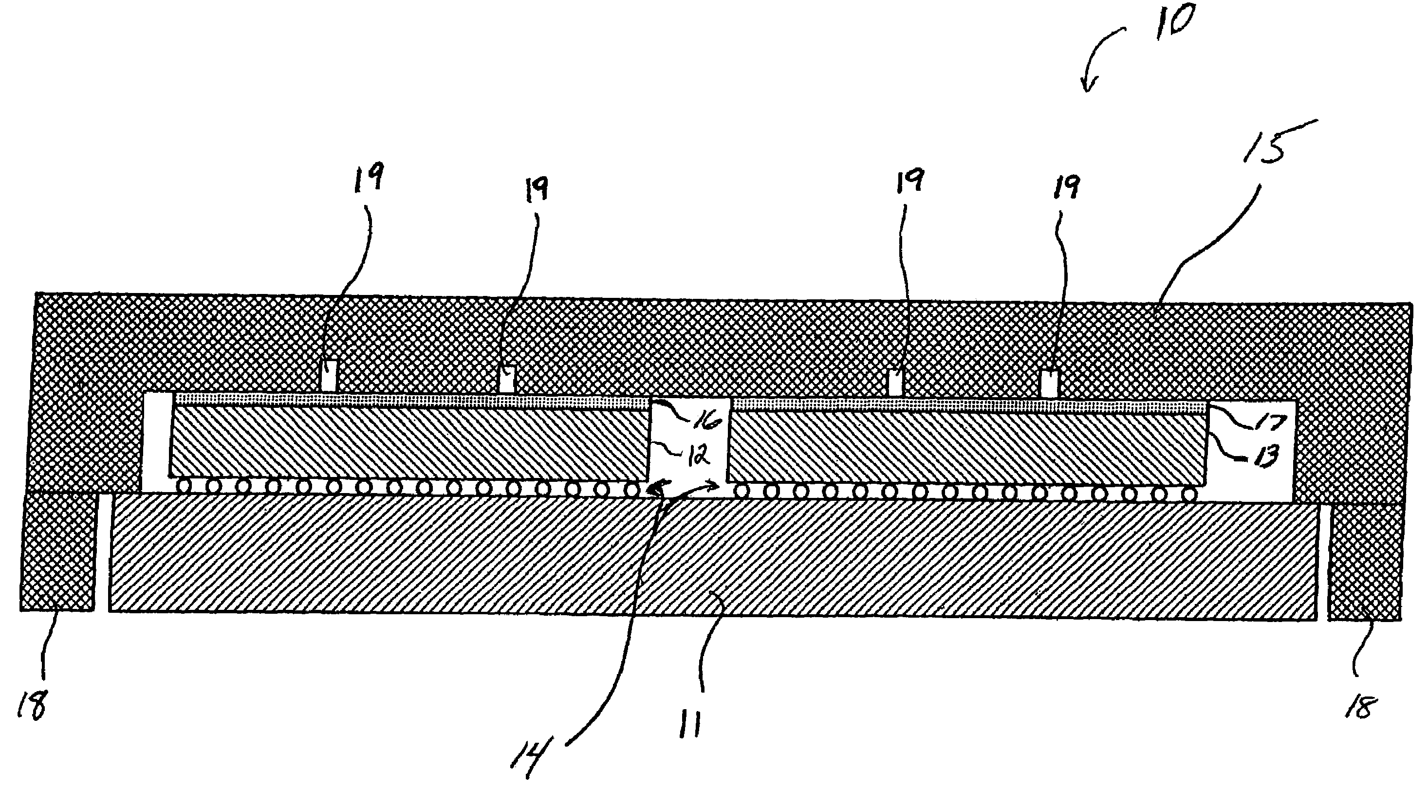
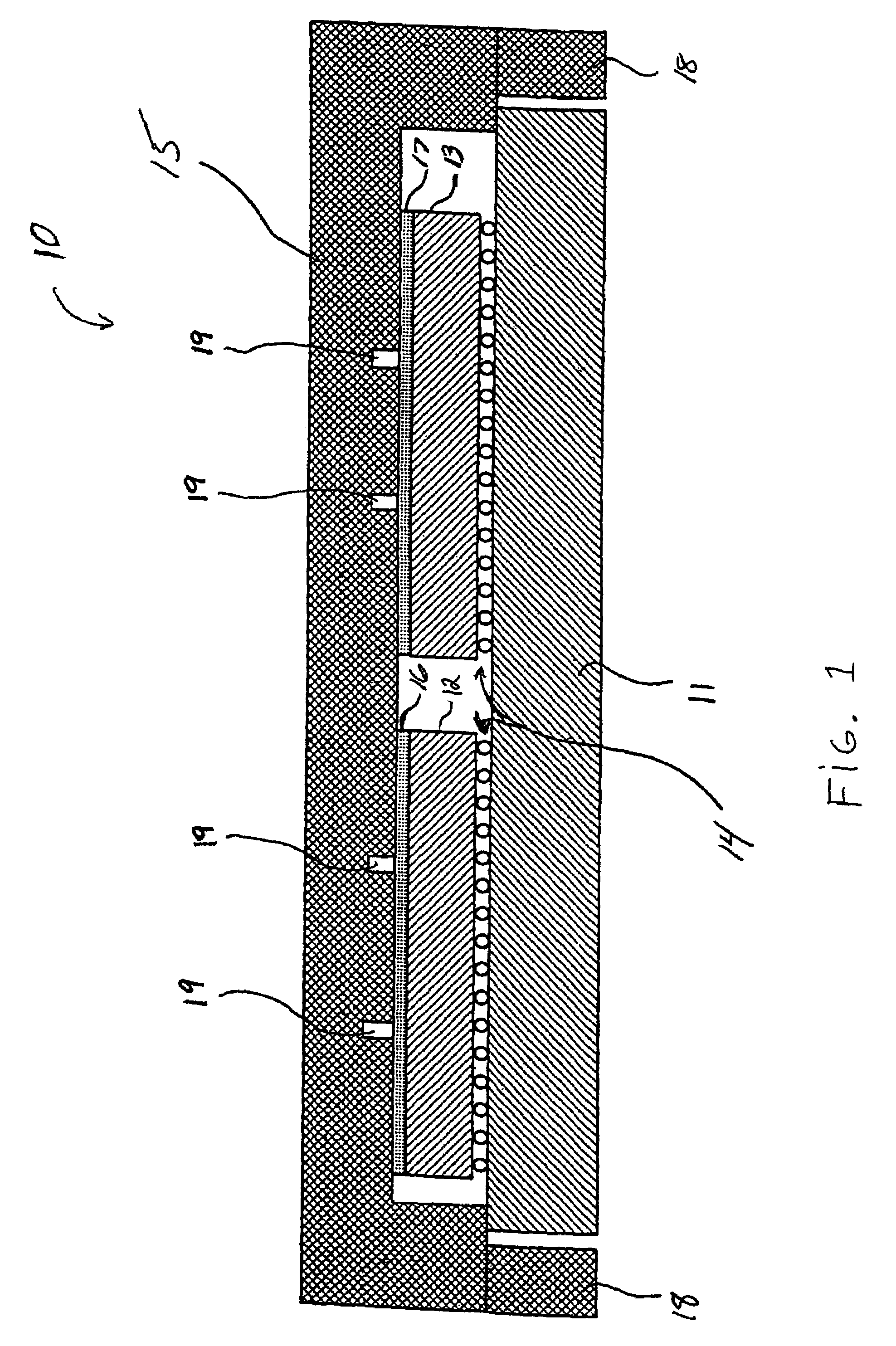
[0020]FIG. 1 schematically illustrates, in general, an apparatus for thermally coupling semiconductor chips to a heat conducting device using compliant thermally conductive material, according to an exemplary embodiment of the invention. In particular, FIG. 1 is a schematic cross-sectional side view of an apparatus (10) (or MCM package) for thermally coupling the back (non-active) surface of semiconductor chips (12) and (13) to a heat conducting device (15) (e.g., package lid, thermal hat, etc.) using compliant thermally conductive material layers (16) and (17) (or TIM (thermal interface material) layers) formed of, e.g., thermal paste. The heat conducting device (15) is rigidly positioned in relation to the back surfaces of the chips (12) and (13). The TIM layers (16) and (17) provide mechanical compliance, as well as a heat conducting path, between the chips (12) and (13) and the heat conducting device (15).

[0021]As explained in further detail below, the apparatus (10) is designed...


PUM


Abstract

The present invention relates generally to apparatus and methods for cooling semiconductor integrated circuit (IC) chip package structures. More specifically, the present invention relates to apparatus and methods for thermally coupling semiconductor chips to a heat conducting device (e.g., copper thermal hat or lid) using a compliant thermally conductive material (e.g., thermal paste), wherein a thermal interface is designed to prevent / inhibit the formation of voids in the compliant thermally conductive material due to the flow of such material in and out from between the chips and the heat conducting device due to thermal cycling.

Description

TECHNICAL FIELD OF THE INVENTION[0001]The present invention relates generally to apparatus and methods for cooling semiconductor integrated circuit (IC) chip package structures. More specifically, the present invention relates to apparatus and methods for thermally interfacing semiconductor chips to a heat conducting device (e.g., thermal hat) using a compliant thermally conductive material (e.g., thermal paste), wherein the thermal interface is designed to prevent the formation of voids in the compliant thermally conductive material.BACKGROUND[0002]In the design and manufacture of semiconductor IC (integrated circuit) chip packages and modules (e.g., SCM (single chip modules) or MCMs (multi-chip modules)), it is imperative to implement mechanisms that can effectively remove heat generated by IC chip devices (such as microprocessors) to ensure continued reliable operation of the devices. Effective heat removal becomes increasingly problematic as chip geometries are scaled down and o...

Claims


Application Information

Patent Timeline
Patent Type & Authority Patents(United States)
IPC IPC(8): H05K7/20H01L23/367
CPCH01L23/42H01L2224/16H01L2224/32057H01L2224/73253H01L2224/83385H01L2924/15311H01L2924/16152H01L2924/10253H01L2924/01019H01L2924/00H01L2924/00011H01L2924/00014H01L2224/0401
Inventor COLGAN, EVAN GEORGEGOTH, GARYSYLVESTER, DEBORAH ANNEZITZ, JEFFREY ALLEN
Owner INT BUSINESS MASCH CORP
Why Eureka
Try Eureka