Pixel circuit, method of driving the same, and electronic apparatus

a technology of pixel circuit and driving current, applied in the direction of identification means, instruments, static indicating devices, etc., to achieve the effect of reducing the dependency on vth of the driving curren

Inactive Publication Date: 2005-05-12
SEIKO EPSON CORP
View PDF6 Cites 34 Cited by
  • Summary
  • Abstract
  • Description
  • Claims
  • Application Information

AI Technical Summary

Benefits of technology

[0017] In the present invention, the gate voltage of the first transistor is previously set to the offset voltage, and the data writing to the capacitor is made in the current-programmed mode. Data to be written is set based on the offset voltage previously set and according to the product of the data current and the supply time thereof. Thus, when the driving current is generated based on data stored in the capacitor, it is possible to reduce a dependency on Vth of the driving current. As a result, even when data writing is lacking, it is possible to generate an uniform driving current, and thus it is possible to set the electro-optical device to have a desirable brightness.

Problems solved by technology

Further, in the case that a current to be programmed in a pixel is very small (when using high efficient EL element or phosphorescence material, the above problem may also occur.

Method used


Image

  • Pixel circuit, method of driving the same, and electronic apparatus
  • Pixel circuit, method of driving the same, and electronic apparatus
  • Pixel circuit, method of driving the same, and electronic apparatus

Examples


first embodiment

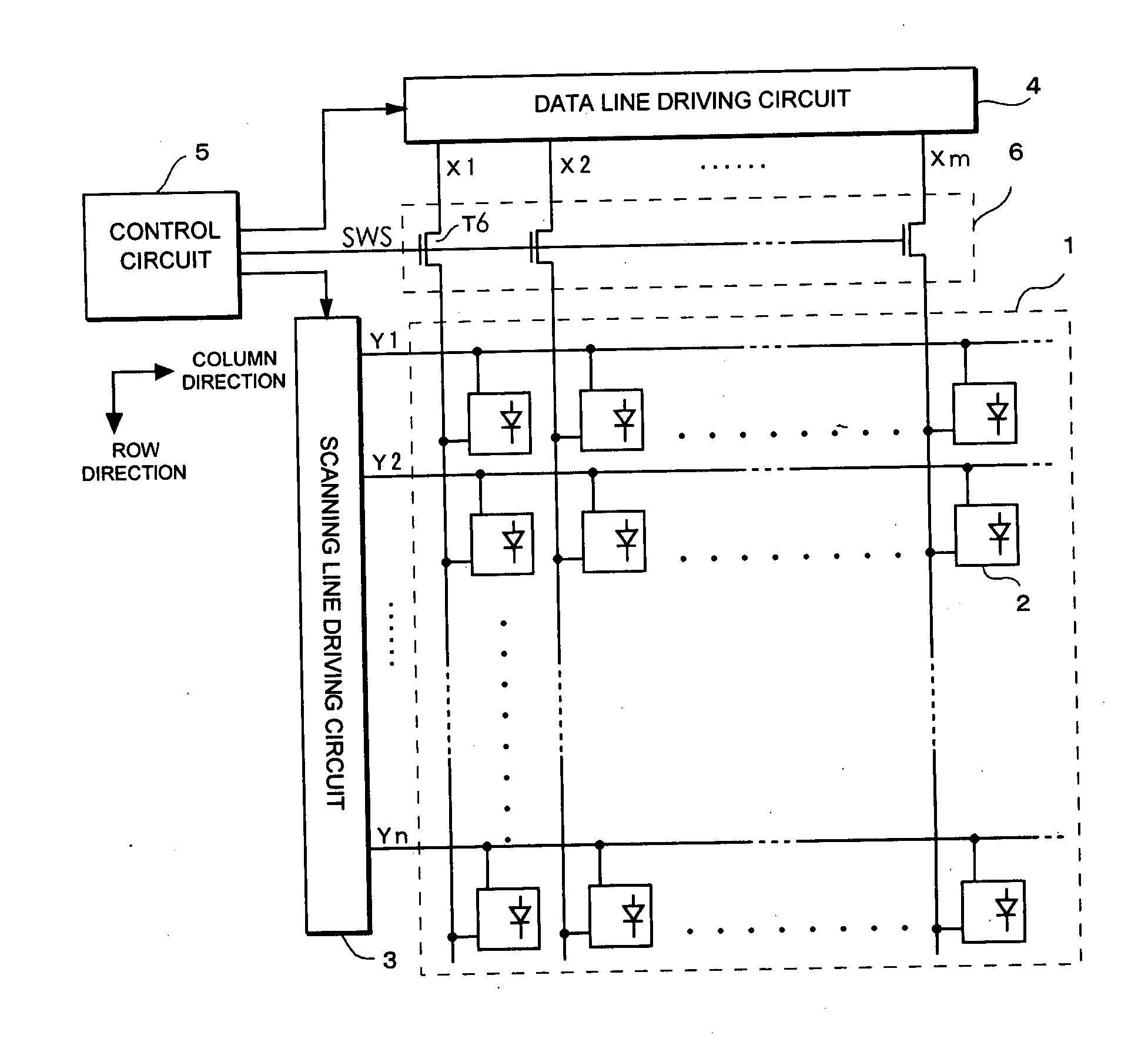
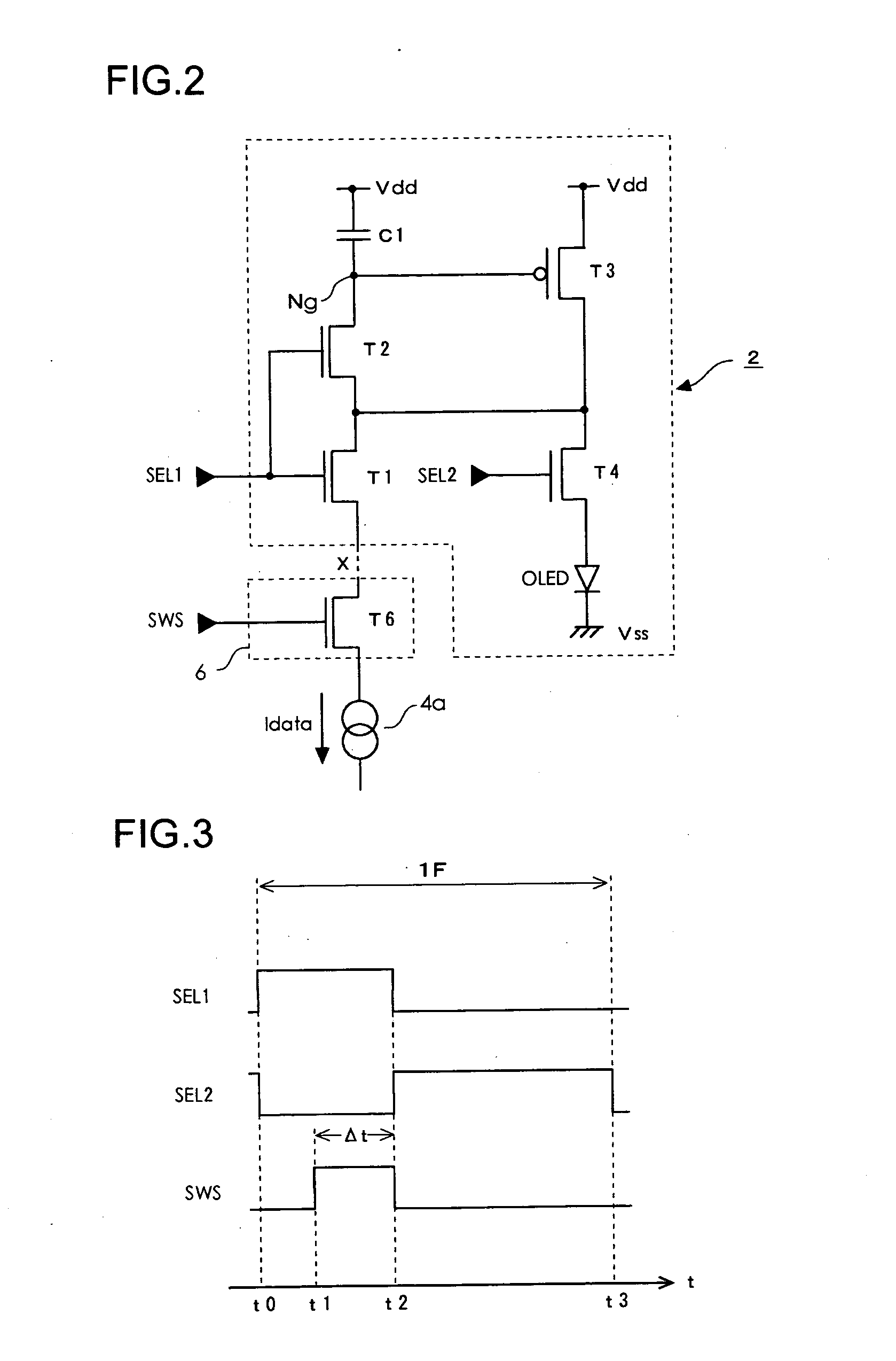
[0035]FIG. 1 is a block diagram showing a configuration of an electro-optical device according to the present embodiment. A display unit 1 is, for example, an active matrix type display panel in which the electro-optical device is driven by a TFT (thin film transistor). In the display unit 1, m dots by n lines of a group of pixels are arranged in a matrix (in a two-dimensional plan view). In the display unit 1, a group of scanning lines Y1 through Yn each extending in a horizontal direction and a group of data lines X1 through Xm each extending in a vertical direction are provided, and pixels 2 are arranged in correspondence with intersections of the scanning lines and the data lines. Moreover, while in a monochromatic panel, one pixel corresponds to one pixel circuit described below, when one pixel comprises three R, G, B sub-pixels like a color panel, one sub-pixel corresponds to one pixel circuit. Further, as regards the configuration of the pixel circuit described below, one sca...

second embodiment

[0049] The present embodiment relates to a technique for regulating the offset voltage (Vdd−Vth) corresponding to the precharge level according to a grayscale level to be displayed, based on the basic configuration of the first embodiment described above. FIG. 5 is a diagram of a pixel circuit according to the present embodiment. The pixel circuit has a feature that a precharge regulation circuit 7 is added to the pixel circuit shown in FIG. 2, and other elements are the same as those of the pixel circuit of FIG. 2. Thus, the descriptions of like elements will be omitted. The precharge regulation circuit 7 comprises a capacitor C2 and a voltage changing circuit 7a for variably setting an output voltage Vp. To one electrode of the capacitor C2, one terminal of the switching transistor T6 constituting a portion of the switching circuit 6 and a connecting terminal with the variable current source 4a are connected. Further, to the other electrode of the capacitor 2, an output terminal o...

third embodiment

[0056] The present embodiment relates to a technique for accelerating the precharge, based on the basic configuration of the first embodiment described above. FIG. 7 is a diagram of a pixel circuit according to the present embodiment. The pixel circuit has two features. The first feature is that a precharge acceleration circuit 8 is added to the pixel circuit shown in FIG. 2. The precharge acceleration circuit 8 is a circuit for outputting a predetermined voltage Vb. The voltage Vb is preferably in vicinities of the above-mentioned offset voltage (Vdd−Vth), but may be less than a voltage such that the driving transistor T3 is turned on, (Vdd−Vth). The second feature is that the switching circuit 6 comprises a group of two switching transistors T6 and T7. The switching transistor T6 is provided between the data line X and the variable current source 4a, and is controlled by a first switching signal SWS1. Further, the switching transistor T7 is provided between the data line X and the...


PUM


Abstract

To control variation in a driving current depending on Vth in a current program mode pixel circuit. In a state in which a variable current source 4a and a transistor T3 are electrically isolated from each other, a gate voltage of the diode-connected transistor T3 is set to an offset voltage (Vdd−Vth) according to a threshold voltage Vth thereof. Next, in a state in which the variable current source 4a and the transistor T3 are electrically connected to each other, data based on the offset voltage and according to a product of a data current Idata and a supply time thereof are written in a capacitor C1 connected to a gate of the transistor T3. And then, a driving current according to data stored in the capacitor C1 is generated by means of the transistor T3, whereby brightness of an organic EL element OLED is set.

Description

BACKGROUND OF THE INVENTION [0001] 1. Field of Invention [0002] The present invention relates to a pixel circuit, a method of driving the same, and electronic apparatus, and more specifically, it relates to a method of compensating Vth in a current-programmed method. [0003] 2. Description of Related Art [0004] Recently, displays using an organic electroluminescent (EL) element draw attention. The organic EL element is one of current-driven type elements in which the brightness is set according to a driving current flowing therethrough. A data supplying method to pixels using the organic EL element includes a voltage-programmed mode in which voltage-based data is supplied to data lines and a current-programmed mode in which current-based data is supplied to the data lines. In the voltage-programmed mode, a problem occurs that variation in a driving current depending on a threshold voltage (hereinafter, referred to as ‘Vth’) of a driving transistor may be caused, but conventionally, t...

Claims


Application Information

Patent Timeline
Patent Type & Authority Applications(United States)
IPC IPC(8): G09F9/30H01L51/50G09G3/12G09G3/20G09G3/30G09G3/32G09G5/00H05B33/00H05B33/04H05B33/14
CPCG09G3/325G09G3/3275G09G2320/0223G09G2310/0248G09G2300/0861G09G3/30G09F9/30H05B33/04
Inventor KASAI, TOSHIYUKI
Owner SEIKO EPSON CORP
Why Eureka
Try Eureka