Failure detection system, failure detection method, and computer program product

Inactive Publication Date: 2005-05-12
KK TOSHIBA
View PDF6 Cites 19 Cited by
  • Summary
  • Abstract
  • Description
  • Claims
  • Application Information

AI Technical Summary

Problems solved by technology

One of the most important problems leading to better productivity in the production of a semiconductor device such as a large-scale integrated circuit (LSI) is to improve a yield rate.
Accordingly, once a failure occurs in the LSI, it is very difficult in general to detect a reason for the failure.
In many cases, the clustering failure is caused by a systematic factor attributable to the manufacturing process, the manufacturing apparatus and the like.
The clustering failure is a major reason for a decrease in the yield rate.
The failure attributable to the manufacturing process, manufacturing apparatus and the like generates a failure pattern inherent in the manufacturing process and the man

Method used


Image

  • Failure detection system, failure detection method, and computer program product
  • Failure detection system, failure detection method, and computer program product
  • Failure detection system, failure detection method, and computer program product

Examples


first embodiment

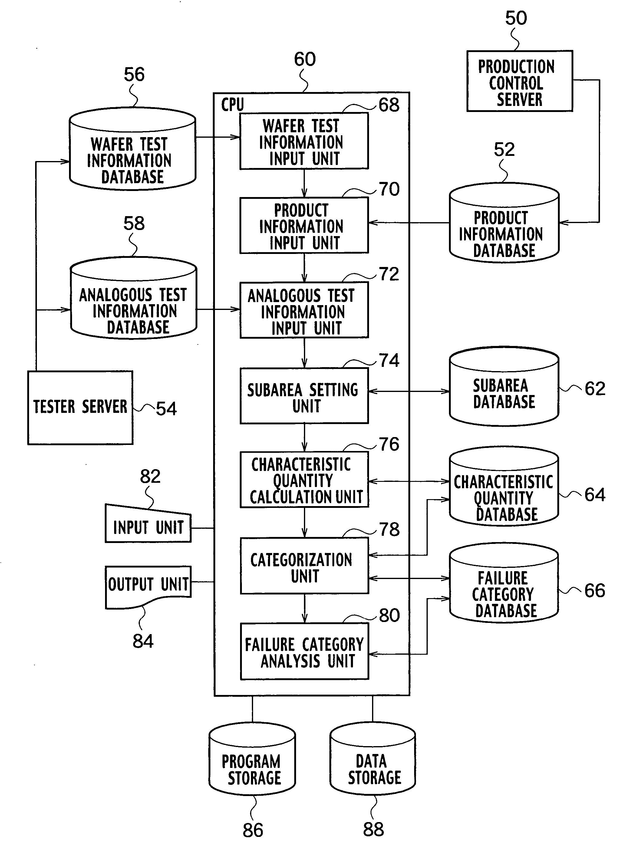
[0040] As shown in FIG. 1, a failure detection system according to a first embodiment of the present invention includes a product information database 52, a wafer test information database 56, an analogous test information database 58, a subarea database 62, a characteristic quantity database 64, a failure category database 66, and a central processing unit (CPU) 60. The product information database 52 is connected to a production control server 50. Moreover, the wafer test information database 56 and the analogous test information database 58 are connected to a tester server 54. An input unit 82, an output unit 84, a program storage 86, and a data storage 88 and the like, are connected to the CPU 60. Furthermore, the CPU 60 includes a wafer test information input unit 68, a product information input unit 70, an analogous test information input unit 72, a subarea setting unit 74, a characteristic quantity calculation unit 76, a categorization unit 78 and a failure category analysis ...

second embodiment

[0077] As shown in FIG. 21, a failure detection system according to a second embodiment of the present invention includes a product information database 52, a wafer test information database 56, an analogous test information database 58, a subarea database 62, a characteristic quantity database 64, a failure category database 66, and a CPU 60a. The product information database 52 is connected to a production control server 50. Moreover, the wafer test information database 56 and the analogous test information database 58 are connected to a tester server 54. An input unit 82, an output unit 84, a program storage 86, and a data storage 88 are connected to the CPU 60a. Furthermore, the CPU 60a includes a wafer test information input unit 68, a product information input unit 70, an analogous test information input unit 72, a subarea setting unit 74, a characteristic quantity calculation unit 76, a categorization unit 78, a failure category analysis unit 80, and a subarea optimization un...


PUM


Abstract

A failure detection system includes a wafer test information input unit which acquires pass/fail maps for wafers for a plurality of types of semiconductor devices, displaying failure chip areas based on results of electrical tests performed on chips; an analogous test information input unit which classifies the electrical tests into analogous electrical tests with regard to analogous failures among the semiconductor devices; a subarea setting unit which assigns subareas common to the types of semiconductor devices on a wafer surface; a characteristic quantity calculation unit which statistically calculates characteristic quantities based on a number of the failure chip areas included in the subareas for each analogous electrical test; and a categorization unit which obtains correlation coefficients between the characteristic quantities corresponding to the subareas, and classifies clustering failure patterns of the failure chip areas into categories by comparing the correlation coefficients with a threshold.

Description

CROSS REFERENCE TO RELATED APPLICATIONS [0001] This application is based upon and claims the benefit of priority from prior Japanese Patent Application P2003-378195 filed on Nov. 7, 2003; the entire contents of which are incorporated by reference herein. BACKGROUND OF THE INVENTION [0002] 1. Field of the Invention [0003] The present invention relates to detection of an abnormality in a manufacturing process of a semiconductor integrated circuit. Particularly, the present invention relates to a failure detection system, a failure detection method and a computer program product for detecting the cause of a clustering failure. [0004] 2. Description of the Related Art [0005] One of the most important problems leading to better productivity in the production of a semiconductor device such as a large-scale integrated circuit (LSI) is to improve a yield rate. In order to improve the yield rate, it is important, by analyzing a yield loss, to analyze a manufacturing process, a manufacturing ...

Claims


Application Information

Patent Timeline
IPC IPC(8): G01R31/26G01R31/01G11C29/00G11C29/56H01L21/66
CPCG01R31/01G11C29/006G11C2029/5604G11C2029/0403G11C29/56
Inventor MATSUSHITA, HIROSHIKADOTA, KENICHISHIOYAMA, YOSHIYUKI
Owner KK TOSHIBA
Why Eureka
Try Eureka