Electrical contacts for molecular electronic transistors

a technology of electronic transistors and electrical contacts, which is applied in the direction of solid-state devices, nano-informatics, semiconductor devices, etc., can solve the problems of increasing the difficulty of further miniaturizing devices via conventional semiconductor fabrication, increasing the cost of associated devices, and consuming very little power, and achieves high cost-effectiveness and large storage capacity.

Active Publication Date: 2005-05-19
AVIRAM ARI
View PDF22 Cites 8 Cited by
  • Summary
  • Abstract
  • Description
  • Claims
  • Application Information

AI Technical Summary

Benefits of technology

[0053] It is another object of the present invention to provide a highly cost-eff...

Problems solved by technology

These very small, specific, sensitive devices provide means for interfacing electrical and chemical systems while consuming very little power.
Generally, with regard to...

Method used


Image

  • Electrical contacts for molecular electronic transistors
  • Electrical contacts for molecular electronic transistors
  • Electrical contacts for molecular electronic transistors

Examples


example 1

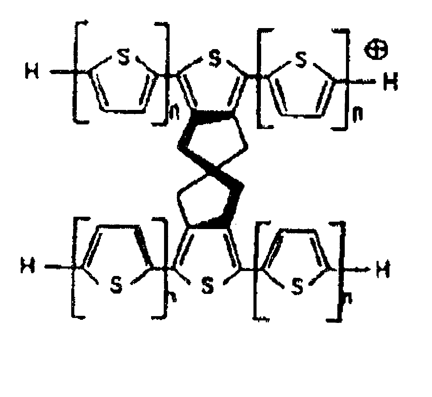
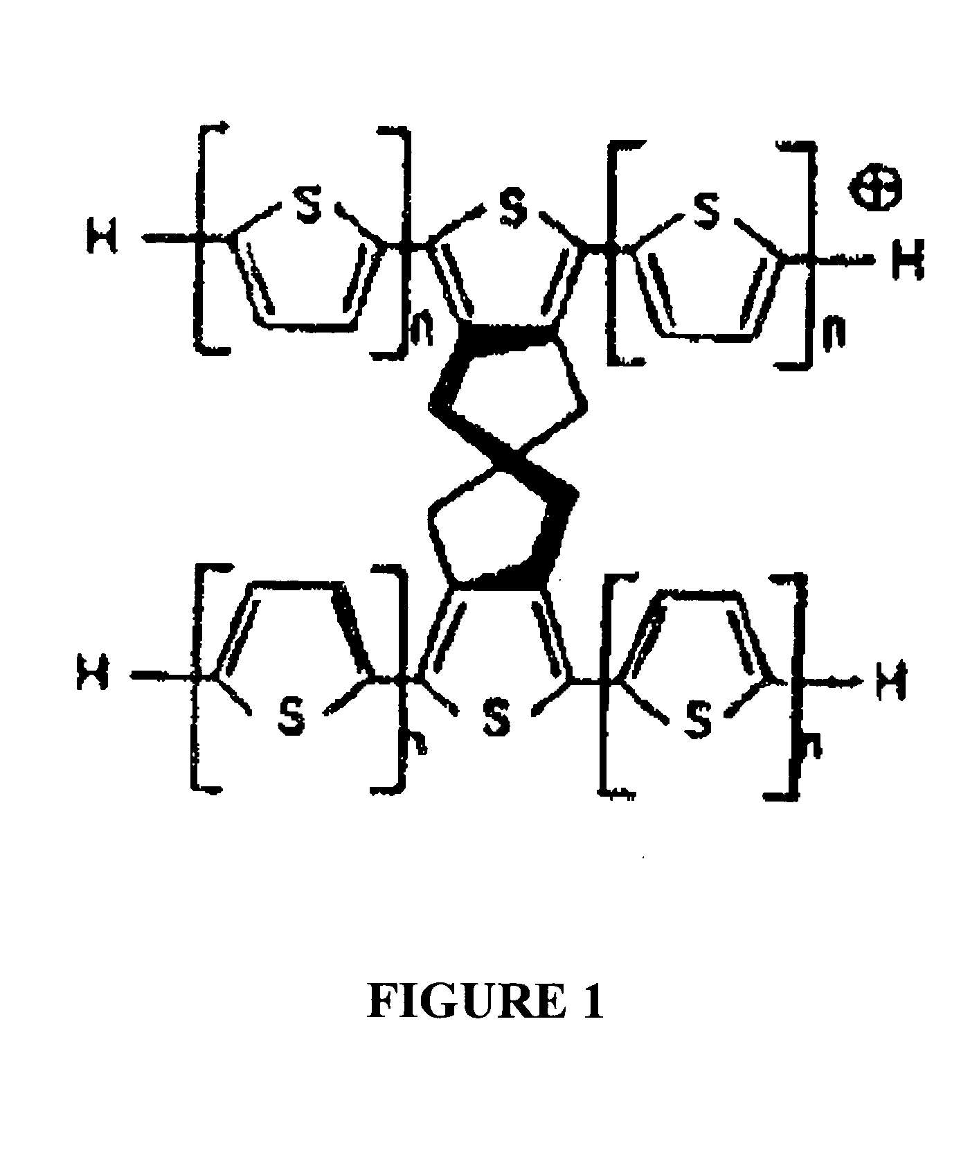
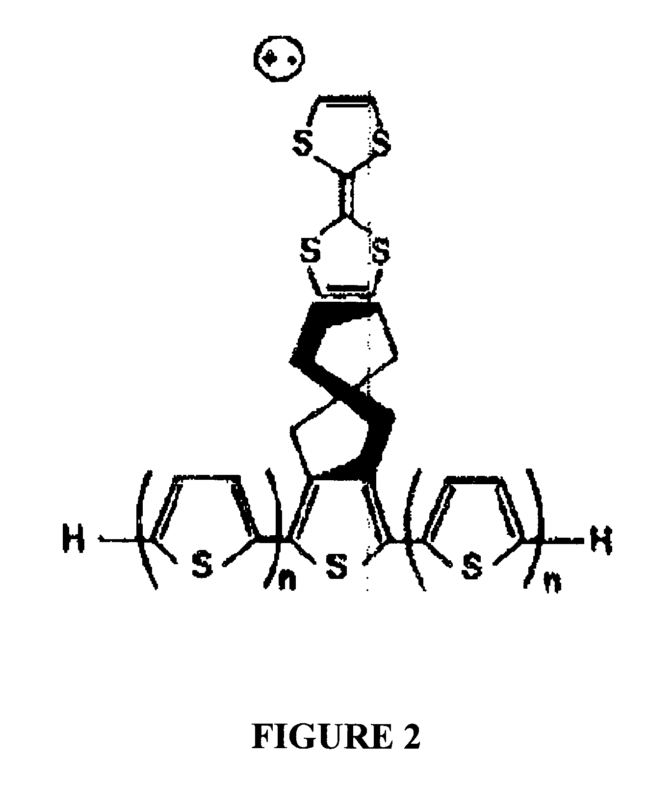
[0071] First, a molecule such as that depicted in FIG. 2 can be “wired” as a transistor by distinguishing between the source / drain metallurgy and the gate metallurgy, and by providing the proper alligator clips to direct the molecule toward the proper connection. The alligator clips on the source / drain chain are —SH groups. The alligator clip on the gate chain is a phosphate group. Initially the oxidation state of the molecule is neutral.

[0072] A metal-electrode pattern is then provided on an insulating surface with gaps in locations where the molecules belong. Importantly, the size of the gap is tailored to fit the length of the molecule. The metallurgy is chosen according to several considerations, including the following:

[0073] The gate electrode is fabricated from aluminum, which couples specifically to the phosphate alligator clip on the molecule (gate chain). The source / drain electrodes are fabricated from platinum in this mode, which couples specifically to the —SH alligato...

example 2

[0075] Second, the molecule depicted in FIG. 2 can be prepared in a doubly-oxidized state, with two electrons missing. In this case, the wiring proceeds much in the manner of that described in EXAMPLE 1. However, the electrochemistry step is that of reduction; as a negative voltage is applied.

example 3

[0076] Next, the circuit is obtained in the same way as described with regard to EXAMPLE 1, in this instance with photochemical oxidation. The oxidation step is accomplished by following the procedure for assembling the circuit that is described in EXAMPLE 1.

[0077] Specifically, the chip is immersed in a concentrated solution containing the molecules shown in FIG. 2, followed by rinsing. Once the molecules are in place, the circuit is preferably immersed in carbon tetrachloride and irradiated with UV radiation. Photochemical oxidation then occurs, and the mixed-valence state is formed.


PUM


Abstract

Electronic circuits based on molecular transistors, generally used in place of semiconductors. More particularly, the invention relates to a unique method of wiring of a three-terminal molecule (or an aggregate thereof) to serve as an electronic transistor, containing a gate electrode, a source electrode, and a drain electrode. The source electrode and drain electrode are fabricated from one metal and the gate electrode is fabricated from another metal. The usage of molecular properties in this context provides significant advantages over the fabrication methods of the prior art.

Description

BACKGROUND OF THE INVENTION [0001] 1. Field of the Invention [0002] The present invention relates to electronic circuits based on molecular transistors, generally used in place of semiconductors. More particularly, the invention relates to a unique method of wiring of a three-terminal molecule (or an aggregate thereof) to serve as an electronic transistor, containing a gate electrode, a source electrode, and a drain electrode. The source electrode and drain electrode are fabricated from one metal and the gate electrode is fabricated from another metal. The usage of molecular properties in this context provides significant advantages over the fabrication methods of the prior art. [0003] 2. Description of the Prior Art [0004] Numerous innovations for electronic circuits have been provided in the prior art that are described as follows. Although these innovations may be suitable for the specific individual purposes to which they address, they differ from the present invention as herein...

Claims


Application Information

Patent Timeline
IPC IPC(8): H01L21/00H01L21/20H01L51/05
CPCB82Y10/00H01L51/0021H01L51/0036Y10S977/936H01L51/0508H01L51/0595H01L51/0051H10K71/60H10K85/113H10K85/611H10K10/46H10K10/701
Inventor AVIRAM, ARI
Owner AVIRAM ARI
Why Eureka
Try Eureka