High value split poly P-resistor with low standard deviation

a polysilicon resistor and standard deviation technology, applied in the direction of diodes, semiconductor devices, electrical devices, etc., can solve the problems of thinned thickness still reducing the standard deviation of resistance, and achieve the effect of improving the control of resistor value, high value and increasing polysilicon resistan

Inactive Publication Date: 2005-05-19
SEMICON COMPONENTS IND LLC
View PDF8 Cites 9 Cited by
  • Summary
  • Abstract
  • Description
  • Claims
  • Application Information

AI Technical Summary

Benefits of technology

[0013] An objective of the present invention is to provide a high value polysilicon resistor requiring an additional single mask step to a typical CMOS, bipolar or BiCMOS process flow. Another objective is to improve the control of the resistor value while increasing the polysilicon resistance, in a particular instance, by more than an order of magnitude.
[0015] In the Leibiger application a second objective of the invention is construction of the high value resistor out of two separately deposited polysilicon layers in such a way that the intrinsic resistor is formed from only one layer, while the resistor ends are formed from two self-aligned stacked layers. This allows the intrinsic resistor to be thinner and more lightly doped to achieve a high sheet resistance value (greater than 2000 ohms per square), while the end polysilicon stack can be thick enough to easily withstand normal processing such as contact etch, silicide formation, or other existing steps. The ends can also be implanted or otherwise doped heavier than the resistor body so that ohmic connections between the poly and the silicide or contact material can be achieved.
[0016] It was found that a reduction in the thickness of the second polysilicon layer, that primarily determines the resistor value in the Leibeiger application, to less than 1000 Angstroms increase the resistance as might be expected, but the thinner layer also significantly reduced the standard deviation of the of the resistance itself. It has also been found that reducing the width of the second layer increased the resistance, as expected, but also increased the standard deviation of the resistance. However, even with a reduced width of the second layer, the thinner thickness still reduced the standard deviation of the resistances.
[0018] where R is the resistance of the structure, ρ is the resistivity (a material property), L is the length of the resistor and A is the cross-sectional area of the resistor. The cross-sectional area (A) is the product of the thickness and width of the resistor. As discussed above, the resistivity of the structure may be increased by changing the dopant concentration. However, as the doping concentration is reduced, the rate of change in resistivity with doping concentration increases dramatically making control of resistivity (and thus resistance) difficult. By reducing the thickness of the structure, the resistance may be increased independently of dopant concentration (reduction in A of Equation 1 above). For identical implant dose, thin POLY has a higher doping concentration (dopant species / unit volume). As such, the resistivity of the layer is lower than thicker POLY. Structures created from this lower resistivity material have much less variation due to the reduced slope in resistivity (FIG. 1) and due to the fact that concentration driven diffusion between the resistor body and the ends is reduced.

Problems solved by technology

However, even with a reduced width of the second layer, the thinner thickness still reduced the standard deviation of the resistances.

Method used


Image

  • High value split poly P-resistor with low standard deviation
  • High value split poly P-resistor with low standard deviation
  • High value split poly P-resistor with low standard deviation

Examples


Embodiment Construction

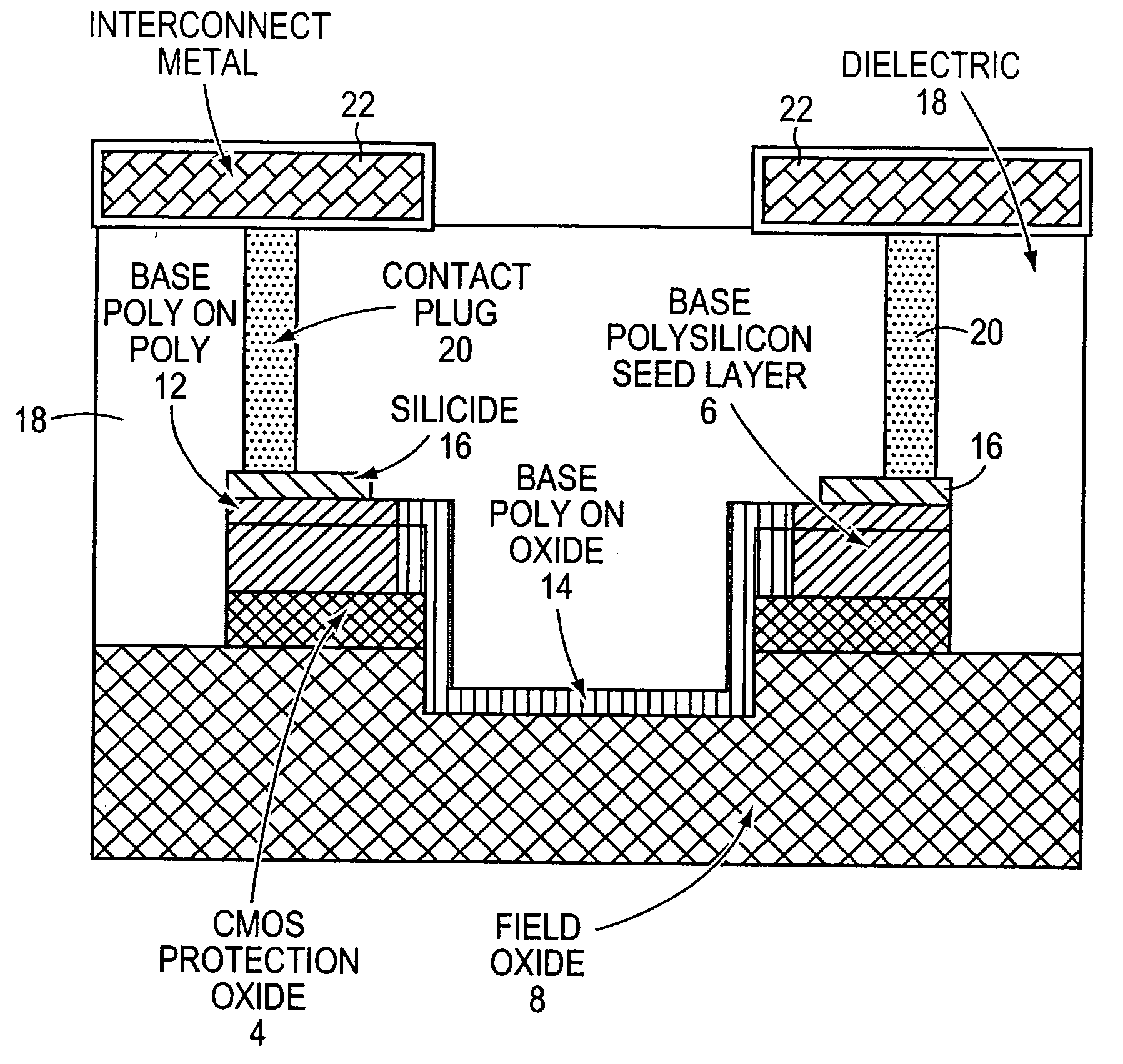
[0029] High value resistors with surface resistivities between 2K ohms / square and 23K ohms / square was built in accordance with the Leibiger application. Some were built with a poly layer that determines the resistivity, see the following discussion, of a thickness of 3700 Angstroms (A). and others were built with the layer thickness of 1000 A. The thicker polysilicon leg was a 300 A a-Si, and a 3400 A polysilicon comprising a 3700 A thickness.

[0030] Another anomaly was observed for resistors with either the 1000 A or the 3700 A layers. If resistors were formed of 50 squares formed with a width of 2 micrometers and a length of 100 micrometers, resistors with five bends had consistently lower standard deviations of resistances compared to identical resistors having no bends or ten bends.

[0031] 12K ohm / square resistors were built with the 1000 A layer that demonstrated and standard deviation of surface resistance of about 4%. In contrast 6K ohm / square resistors made identically excep...


PUM


Abstract

A resistor structure is disclosed that is constructed out of two layers of polysilicon. The intrinsic device is made using the top layer which is either a dedicated deposition, or formed as part of an existing process step such as a base epi growth in a BiCMOS flow. This poly layer can be made with a relatively high (greater than 2000 ohms per square) sheet resistance by appropriate scaling of the implant dose or by insitu doping methods. In this invention this layer is arranged to be about 1000 A or less thick. Such a resistor form with this thickness has been shown to demonstrate a better standard deviation of resistance compared to resistors made with a thicker layer. Additionally, practical resistors made in elongated forms demonstrate better standard deviations of resistance when five bends were incorporated into the form. The resistor ends are formed by the addition of a bottom poly layer in a self aligned manner with a deposition that may already be part of the process sequence. The end result is that the intrinsic resistor body is formed of a single poly layer, while the ends are created out of two layers. These ends are thick enough so that standard silicide and contact etch processing may be added to the structure without special care. In addition, dedicated or already available implants may be incorporated into the resistor ends to ensure ohmic contacts from polysilicon to the silicide or the contact metal are achieved. These steps can produce an easily fabricated resistor structure with consistent, low resistance, ohmic end contacts, and intrinsic resistance of greater than 2000 ohms per square.

Description

CROSS REFERENCE TO RELATED APPLICATIONS [0001] The present application is a divisional of commonly assigned copending, allowed U.S. patent application Ser. No. 10 / 355,317, which was filed on Jan. 31, 2003, of common title and inventorship with the present invention, and which is hereby incorporated by reference. Priority is claimed from this co-pending application. [0002] This application is also related to a patent entitled High Value Polysilicon Resistor, by Steven M. Leibiger, U.S. Pat. No. 6,700,474, which was issued on Mar. 2, 2004, and commonly owned with the present application. This patent of Mr. Leibiger is hereby incorporated herein by reference.BACKGROUND OF THE INVENTION [0003] 1. Field of the Invention [0004] The present invention relates to a structure and process for forming polysilicon resistors on semiconductor substrates, and more particularly to dual layer polysilicon high value resistor structures. [0005] 2. Background Information [0006] Forming high value polysi...

Claims


Application Information

Patent Timeline
Patent Type & Authority Applications(United States)
IPC IPC(8): H01L21/02H01L21/8249H01L27/06H01L27/08
CPCH01L21/8249H01L28/20H01L27/0802H01L27/0635H01L27/04
Inventor OLSON, JAMES MICHAEL
Owner SEMICON COMPONENTS IND LLC
Why Eureka
Try Eureka