High-efficiency radiating device

a radiation emitting device and high-efficiency technology, applied in the direction of semiconductor devices, basic electric elements, electrical equipment, etc., can solve the problems of reducing the efficiency of the total light emission of the device, inability to integrate in large arrays, and slowness in the inherently slow process, so as to achieve high radiation emission efficiency and reduce the power consumption of the device

Inactive Publication Date: 2005-05-26
SIGNIFY HLDG BV
View PDF24 Cites 54 Cited by
  • Summary
  • Abstract
  • Description
  • Claims
  • Application Information

AI Technical Summary

Benefits of technology

[0031] In an object of the present invention radiation, preferably light, emitting devices and methods of making such devices are disclosed that have a high radiation emission efficiency. According to this aspect of the invention the outcoupling efficiency of radiation, preferably light, emitting devices is improved, which leads to a reduced power consumption of the devices for a given radiation output power.

Problems solved by technology

The problem with this technique is that it is inherently slow, because one has to wait for multiple re-absorptions and re-emissions.
Thus there is a problem of making highly efficient light emitting devices as the recombination losses of the charge carriers decrease the efficiency of the total light emission of the devices.
Such devices therefore are not suitable for integration in large arrays.
Also, their large area results in a large capacitance, and therefore slow operation.
Thus the prior art fails to disclose highly efficient light-emitting devices that can be integrated as small devices in a dense array of light emitting devices.

Method used


Image

  • High-efficiency radiating device
  • High-efficiency radiating device
  • High-efficiency radiating device

Examples


Embodiment Construction

[0063] For the purpose of teaching of the invention, preferred embodiments of the method and devices of the invention are described in the sequel. It will be apparent to the person skilled in the art that other alternative and equivalent embodiments of the invention can be conceived and reduced to practice without departing form the true spirit of the invention, the scope of the invention being limited only by the appended claims.

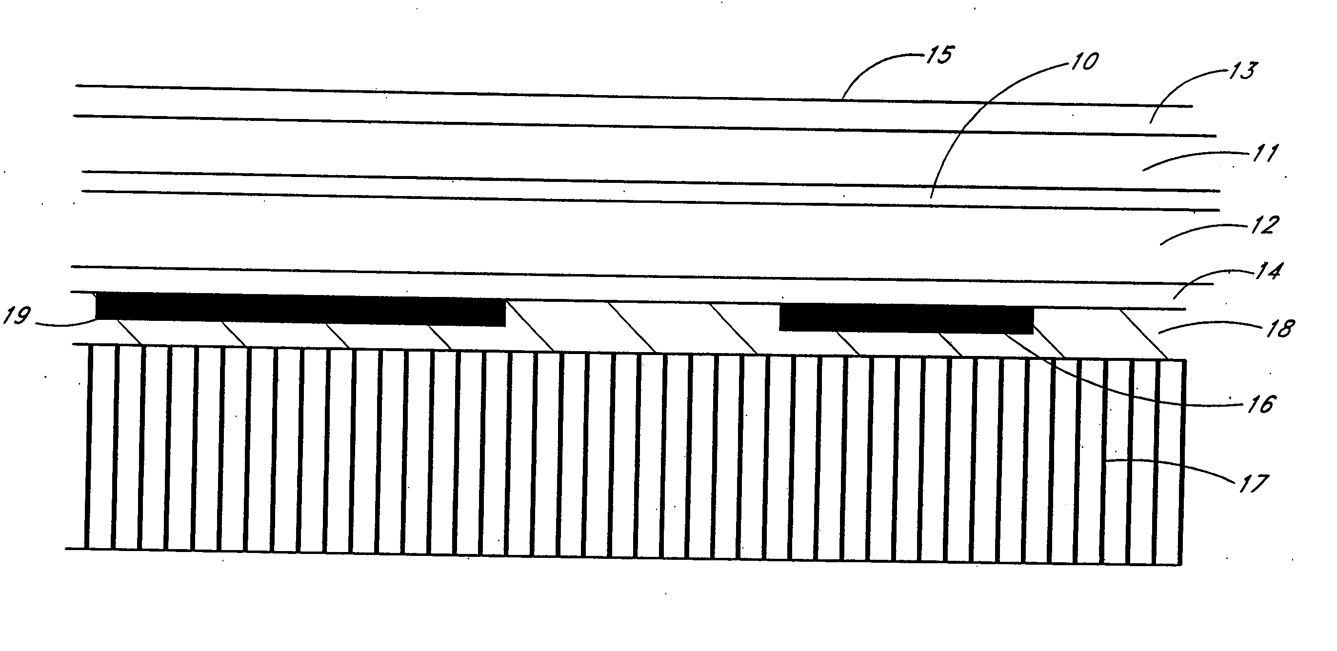
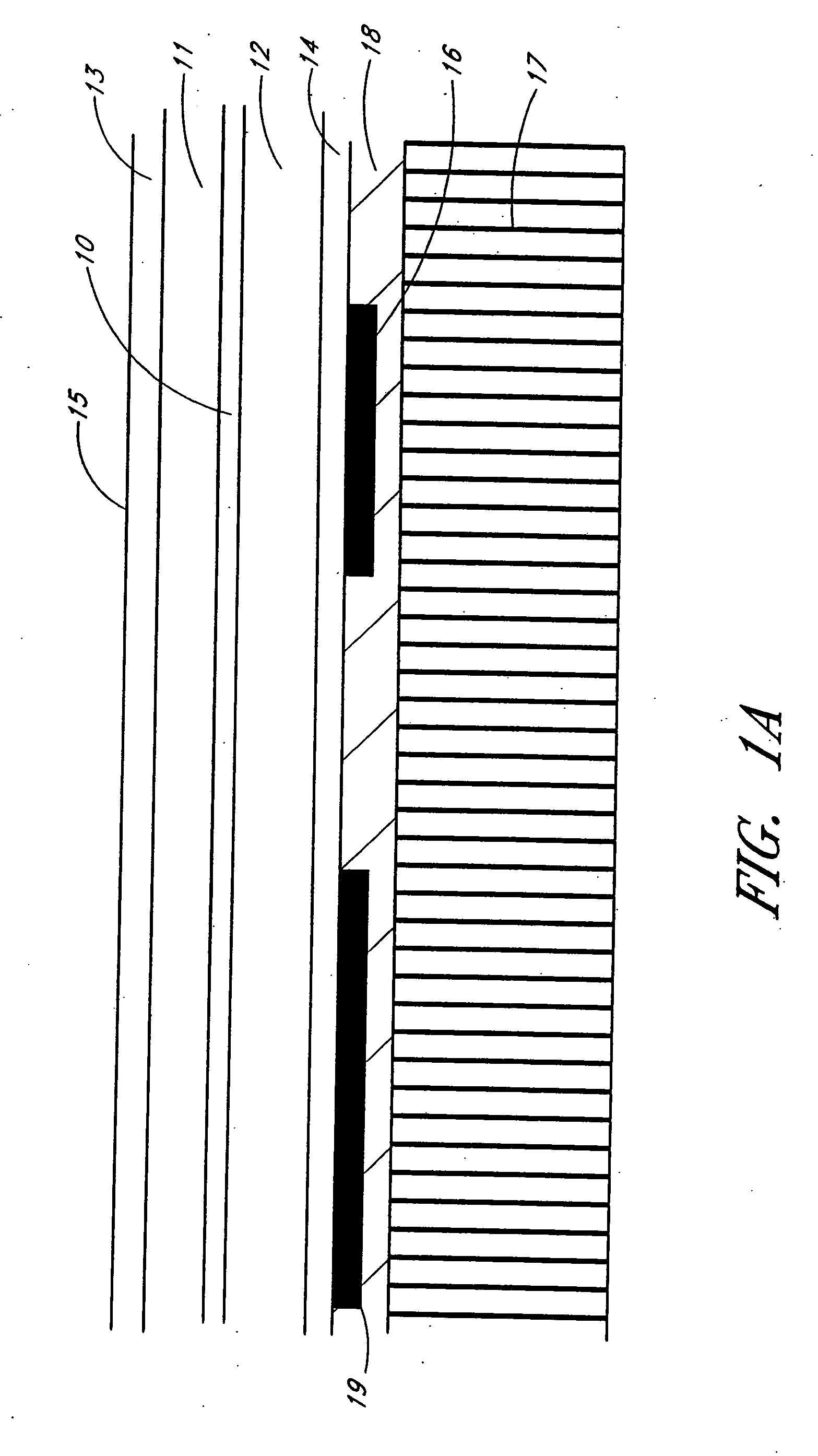
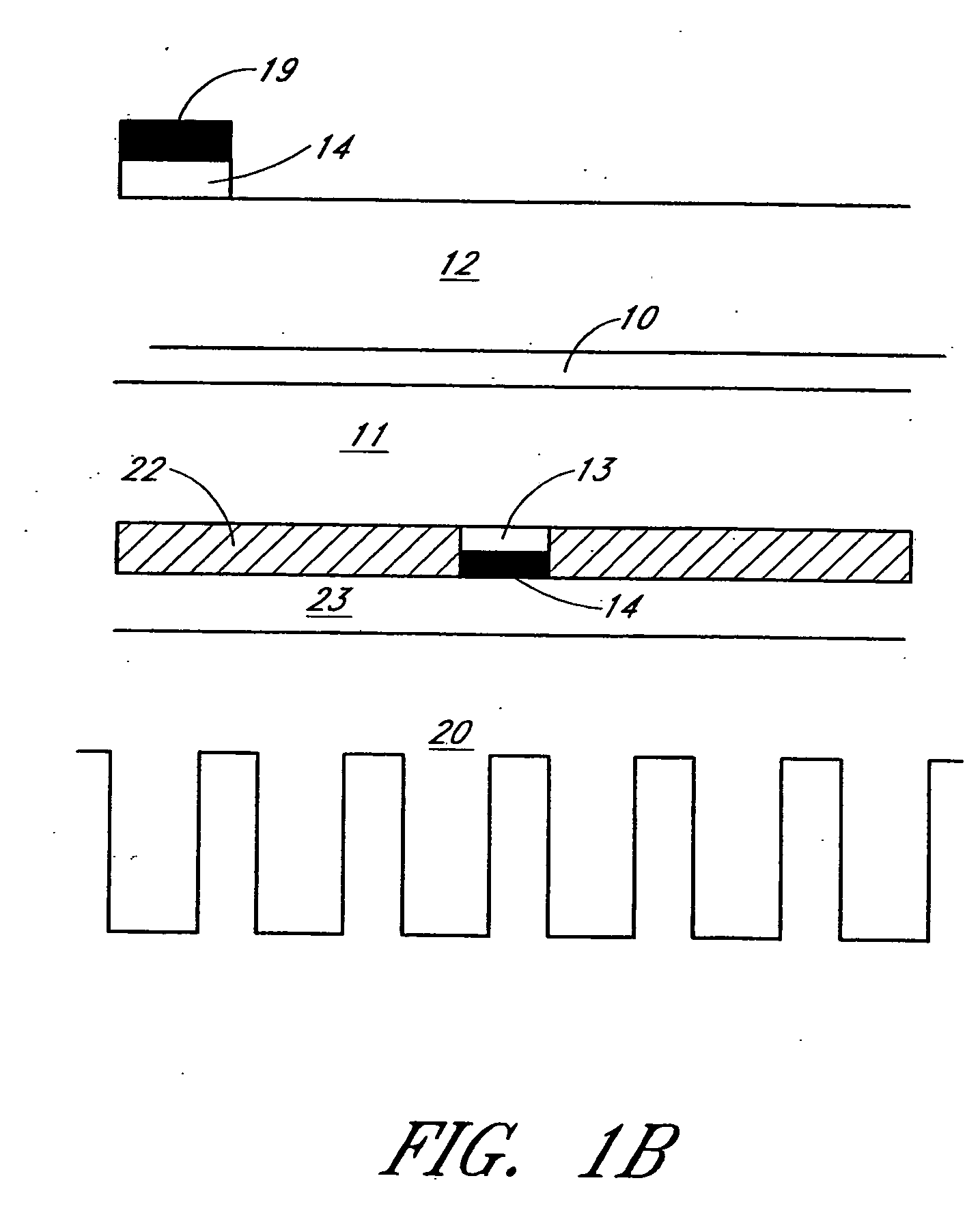
[0064]FIG. 1a shows the layer structure of a light-emitting diode (LED) according to an embodiment of a device of the present invention. This layer structure will be assumed for the devices disclosed in this detailed description of the invention. A layer structure is shown and the layers are made in semiconductor material, preferably III-V semiconductor material and the different layers can be made of different semiconductors. The layers can be epitaxially grown or can be deposited on a substrate. The substrate whereon the layers are made is removed and th...


PUM


Abstract

A device emits radiation at a predetermined wavelength. The device includes a light-emitting diode (LED) which generates the radiation. The device further includes at least one edge having a substantially random diffraction grating structure in radiative communication with the LED.

Description

CLAIM OF PRIORITY [0001] This application is a continuation of U.S. patent application Ser. No. 10 / 272,690, filed Oct. 16, 2002, which is a divisional of U.S. patent application Ser. No. 09 / 360,505, filed on Jul. 26, 1999, issued as U.S. Pat. No. 6,504,180 on Jan. 7, 2003, and which claims the benefit of priority under 35 U.S.C. § 119(e) from U.S. Provisional Application No. 60 / 131,358, filed Apr. 28, 1999, and which also claims the benefit of priority from EPO Applications EP 988701645, filed Jul. 28, 1998; EP 988702338, filed Oct. 30, 1998; and EP 988702528, filed Nov. 13, 1998.FIELD OF THE INVENTION [0002] The present invention is related to the field of radiation emitting devices. More in particular semiconductor devices that emit light at a predetermined wavelength with a high efficiency are disclosed. A method of making such devices and applications of the devices are also disclosed. BACKGROUND OF THE INVENTION [0003] Semiconductor devices that can emit non-coherent or coheren...

Claims


Application Information

Patent Timeline
Patent Type & Authority Applications(United States)
IPC IPC(8): H01L33/02H01L33/08H01L33/20H01L33/22H01L33/46
CPCH01L33/025H01L33/08H01L33/46H01L33/22H01L33/20
Inventor HEREMANS, PAULKUIJK, MAARTENWINDISCH, REINERBORGHS, GUSTAAF
Owner SIGNIFY HLDG BV
Why Eureka
Try Eureka