Interconnector, method for manufacturing a plasma display device using the same, and a plasma display device with the same

a plasma display panel and interconnector technology, applied in the direction of connection contact material, identification means, instruments, etc., can solve the problems of bursting, damage, or other damage to the insulation encapsulation,

Inactive Publication Date: 2005-05-26
SAMSUNG SDI CO LTD
View PDF8 Cites 21 Cited by
  • Summary
  • Abstract
  • Description
  • Claims
  • Application Information

AI Technical Summary

Benefits of technology

[0010] One aspect of the present invention provides a plasma display device in which improved interconnections prevent neighboring connecting terminal portions of an FPC and electrodes of a PDP from short-circuiting.

Problems solved by technology

In some of the pellets, the insulating encapsulation may be broken, burst, or otherwise damaged or removed.

Method used


Image

  • Interconnector, method for manufacturing a plasma display device using the same, and a plasma display device with the same
  • Interconnector, method for manufacturing a plasma display device using the same, and a plasma display device with the same
  • Interconnector, method for manufacturing a plasma display device using the same, and a plasma display device with the same

Examples


second embodiment

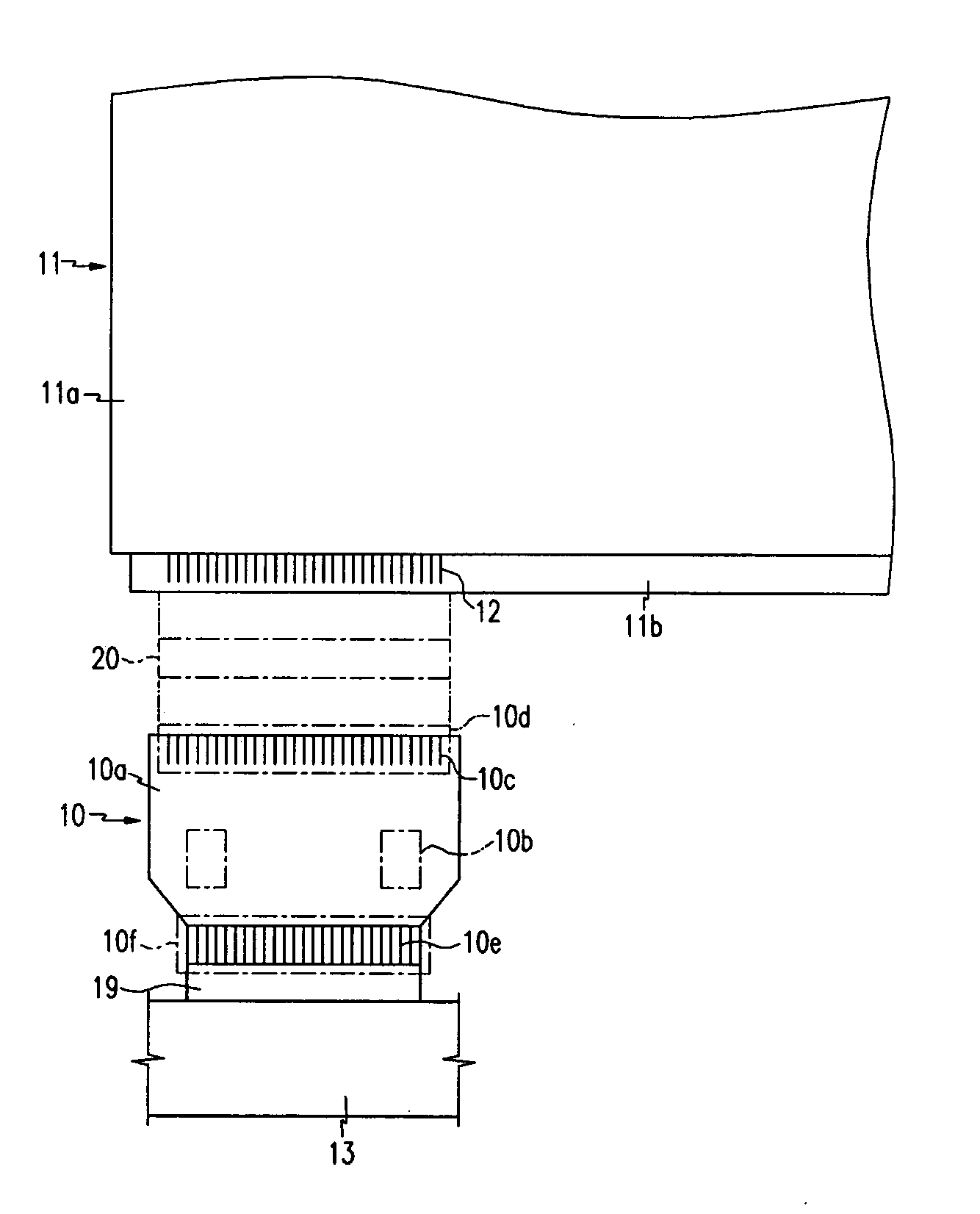
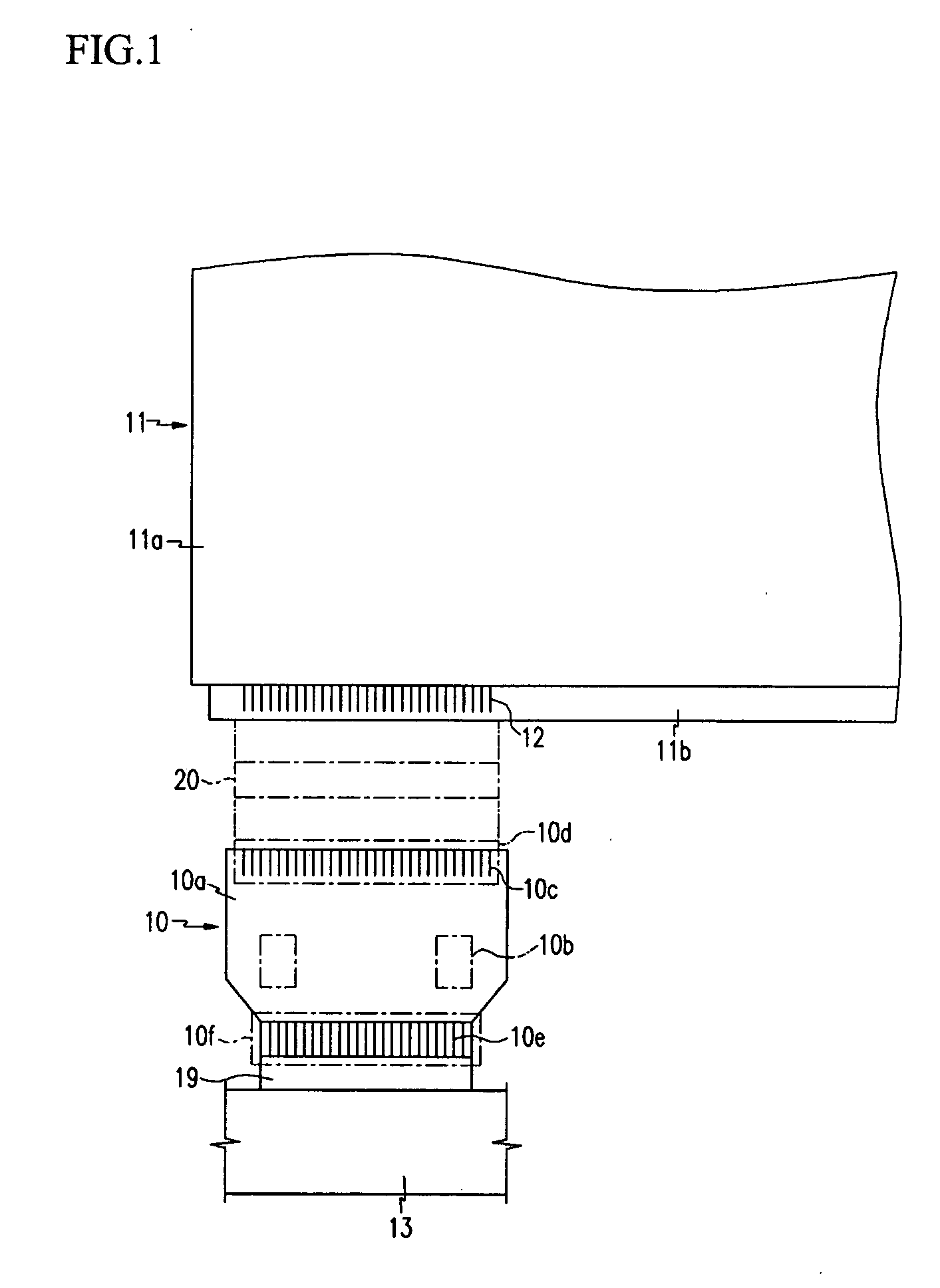
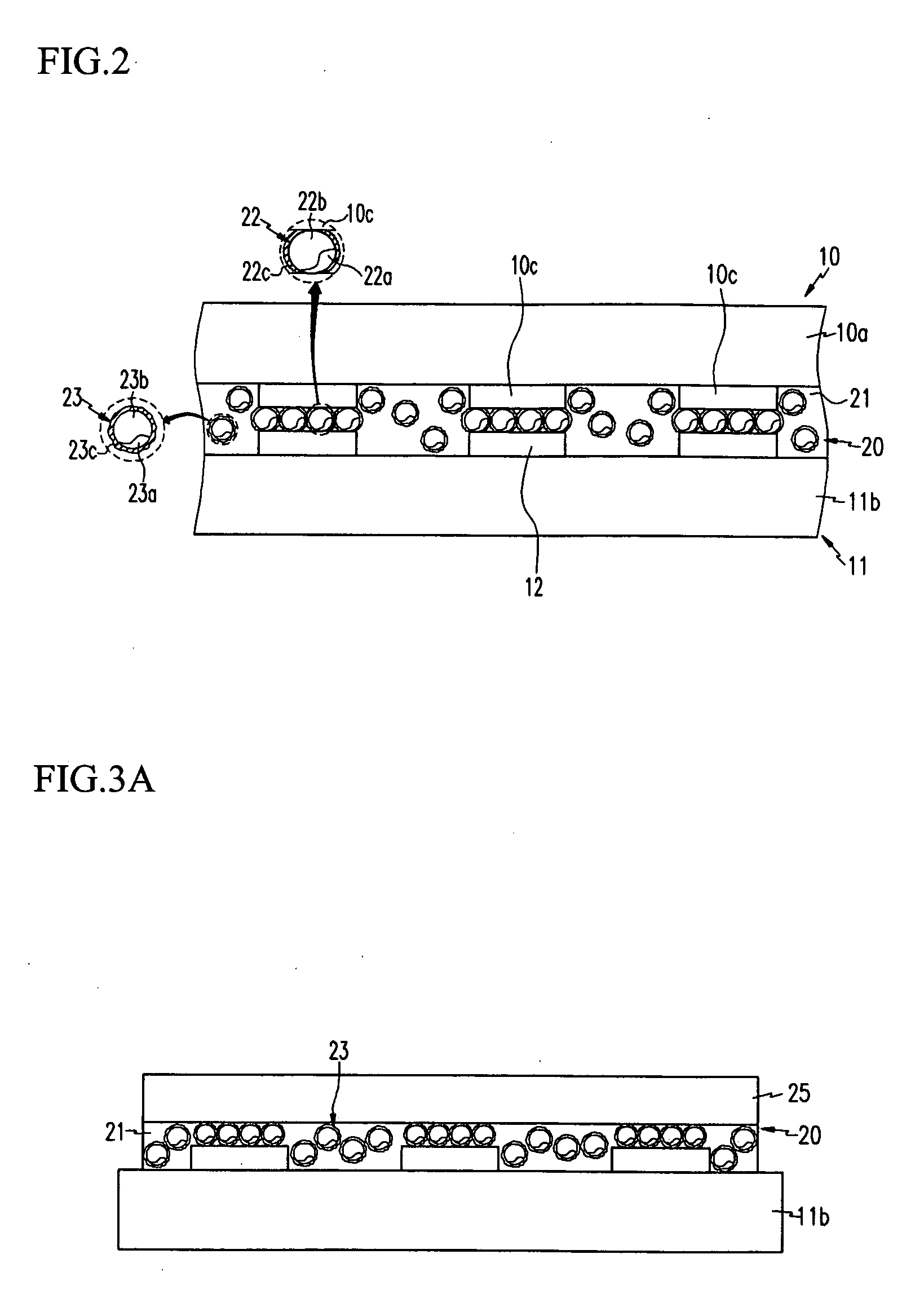
[0048] As shown in FIG. 4, in the present invention, an interconnecter 40 used to electrically connect the PDP 11 with the connecter 10 may include conductive pellets 41 substantially interposed between the connecting wiring 10c of the connecter 20 and the electrodes 12, and non-conductive particles 42 substantially dispersed in the region of the connecter 20 that is not between the connecting wiring 10c of the connecter 20 and the electrodes 12. The non-conductive particles 42 may have a different size than the conductive pellets 41. Here, a plurality of the conductive pellets 41 and non-conductive particles 42 may be dispersed in the adhesive layer 41 in the same manner as discussed above.

[0049] The conductive pellets 41 and the non-conductive particles 42 may have substantially spherical (including ellipsoidal and the like) shapes, and the conductive pellets 41 may preferably have a size of about 4 to about 8 μm while the non-conductive particles 42 may have a size of about 1 to ...

third embodiment

[0054] In the third embodiment, projections 55 may project from either the connecting wiring 10c or the electrode 12 (or both) to electrically connect them. The projections 55 may project from the connecting wiring 10c, and may be formed from a conductive material such as, for example, Au, Ni, or the like. The projections 55 may be configured such that they have a smaller cross-section the closer they are to the driving electrodes 12. Alternatively, the projections 55 may project from the electrodes 12, with an increasingly smaller cross-section toward the wiring 10c.

[0055] Also, in order to connect the electrodes 12 of PDP 11 with the wiring 10c of the connecter using the interconnecter 50 and the projections 55, the thermo-compression method using the pressing device may be used as discussed above.

[0056] In the third embodiment, when connecting the electrodes 12 with the wiring 10c by means of the thermo-compression method, the non-conductive particles 52 can be moved to the reg...


PUM

PropertyMeasurementUnit
sizeaaaaaaaaaa
sizeaaaaaaaaaa
conductiveaaaaaaaaaa

Abstract

A plasma display device may include a plasma display panel, a driving circuit portion for driving the plasma display panel, a connecter for electrically connecting electrodes of the plasma display panel with the driving circuit portion, and an interconnecter for electrically connecting the connecter with the plasma display panel. The interconnecter may include an adhesive layer, a plurality of conductive pellets, and a plurality of non-conductive pellets dispersed in the adhesive layer. The conductive pellets may be positioned substantially within a first region where the wiring of the connecter overlaps the electrodes of the plasma display panel. The non-conductive pellets may be positioned substantially at least at a second region other than the first region in the adhesive layer.

Description

CROSS-REFERENCE TO RELATED APPLICATIONS [0001] This application claims priority to and the benefit of Korean Patent Application No. 10-2003-0074667 filed on Oct. 24, 2003, the entirety of which is incorporated by reference. BACKGROUND OF THE INVENTION [0002] 1. Field of the Invention [0003] The present invention relates to a plasma display device, and more particularly to a structure for electrically connecting a plasma display panel with a driving circuit portion. [0004] 2. Description of the Related Art [0005] Electrodes (for example, address electrodes) on the rear surface of a plasma display panel (PDP) electrically can connect with a driving circuit portion through a connecter (for example, a Flexible Printed Circuit (FPC)). The connecter can have a driver IC for applying an address voltage to the electrodes of the PDP in response to a control signal generated from a driving circuit portion. This address voltage may be applied to selectively form a wall voltage in each of pixel...

Claims


Application Information

Patent Timeline
Patent Type & Authority Applications(United States)
IPC IPC(8): C09J11/00C09J201/00G09F9/00H01J17/16H01J17/49H01R4/04H01R11/01H01R43/00H05K1/14H05K3/30H05K3/32H05K3/36
CPCH01J2211/46H01R4/04H01R12/62H05K1/147H05K3/305H05K3/323H05K2203/1189H05K2201/0212H05K2201/0221H05K2201/0224H05K2201/0233H05K2201/0367H05K2201/10977H05K3/361H01J11/46H01J11/48
Inventor JEONG, YOUNG-CHULKIM, EUN-GONKIM, KI-JUNG
Owner SAMSUNG SDI CO LTD
Why Eureka
Try Eureka