Integrated circuit with improved interconnect structure and process for making same

a technology of integrated circuits and interconnects, applied in the direction of semiconductor devices, semiconductor/solid-state device details, electrical devices, etc., can solve the problems of limiting the size of the area that can become small using conventional processes, high processing costs, poor yield, etc., to reduce cycle time, reduce wafer cycle time, cost-effective

Inactive Publication Date: 2005-01-04
UNITED MICROELECTRONICS CORP
View PDF34 Cites 19 Cited by
  • Summary
  • Abstract
  • Description
  • Claims
  • Application Information

AI Technical Summary

Benefits of technology

Another object of the present invention is to provide an interconnect / packaging structure and method that is simple, cost-effective, fast, and that does not require the critical resources of a conventional semiconductor fab to perform;
A related object is to provide an interconnect and packaging method that can be can be completed before normal wafer processing operations were undertaken to reduce wafer cycle time.
Although the inventions are described below in a preferred embodiment, it will be apparent to those skilled in the art the present invention would be beneficially used in many environments where it is necessary to provide dense I / O interconnect structures, or where it is advantageous to reduce cycle time by providing chip scale packaging to a die even before normal processing operations are begun.

Problems solved by technology

This approach, however, suffers from extremely high processing costs, and very poor yield.
However, there is a limit to how small this area can become using conventional processes, because the pads have to be large enough to accommodate a wire bond, or a flip chip type solder bump.
Thus, there is inevitably a large amount of surface area, otherwise usable for forming electronic circuits, that is wasted in a chip scale type package as shown in FIG.
The vias, appear to be limited to connecting any circuits to a groundplane, however (as evidenced by the single metallization layer shown at the backside of the substrate) and not for connecting such circuits to another circuit (or set of circuits).
It is apparent that this approach, too, is commercially impractical for conventional processing because the fabricating steps are complicated.
None of the above references, nonetheless, appear to address the problem of how to optimize the usable chip surface area, or how to minimize interconnect areas required to contact other chips.
While certain patents issued to Tessera, Inc. are directed generally to this problem (see e.g., U.S. Pat. Nos. 5,148,265; 5,148,266; 5,258,330; and 5,548,091—all of which are hereby incorporated by reference) the solution they proposed involves what is conventionally known as an “interposer,” and the manufacturing operations required to implement this flexible intervening layer (between surface contacts and a ball grid array) are extremely complex.
It is apparent that as chip die sizes become smaller, the design of interconnect areas, including pad shape, size, and placement will become more and more critical, and, at one point, will probably be the limiting factor in chip scale packaging.
A related problem in semiconductor manufacturing is the fact that at least some portion of the interconnect / packaging operations take place within the main fabrication facility, and this is non-optimal for a number of reasons.
First, it is not cost effective, because in general fab space is extremely limited, and equipment, labor and overhead costs are quite high in that environment.
Second, if packaging / interconnect processing steps are set up as part of the normal manufacturing cycle within the fab, they can impact wafer throughput (cycle time) considerably, because they are typically slow operations.

Method used


Image

  • Integrated circuit with improved interconnect structure and process for making same
  • Integrated circuit with improved interconnect structure and process for making same
  • Integrated circuit with improved interconnect structure and process for making same

Examples


second embodiment

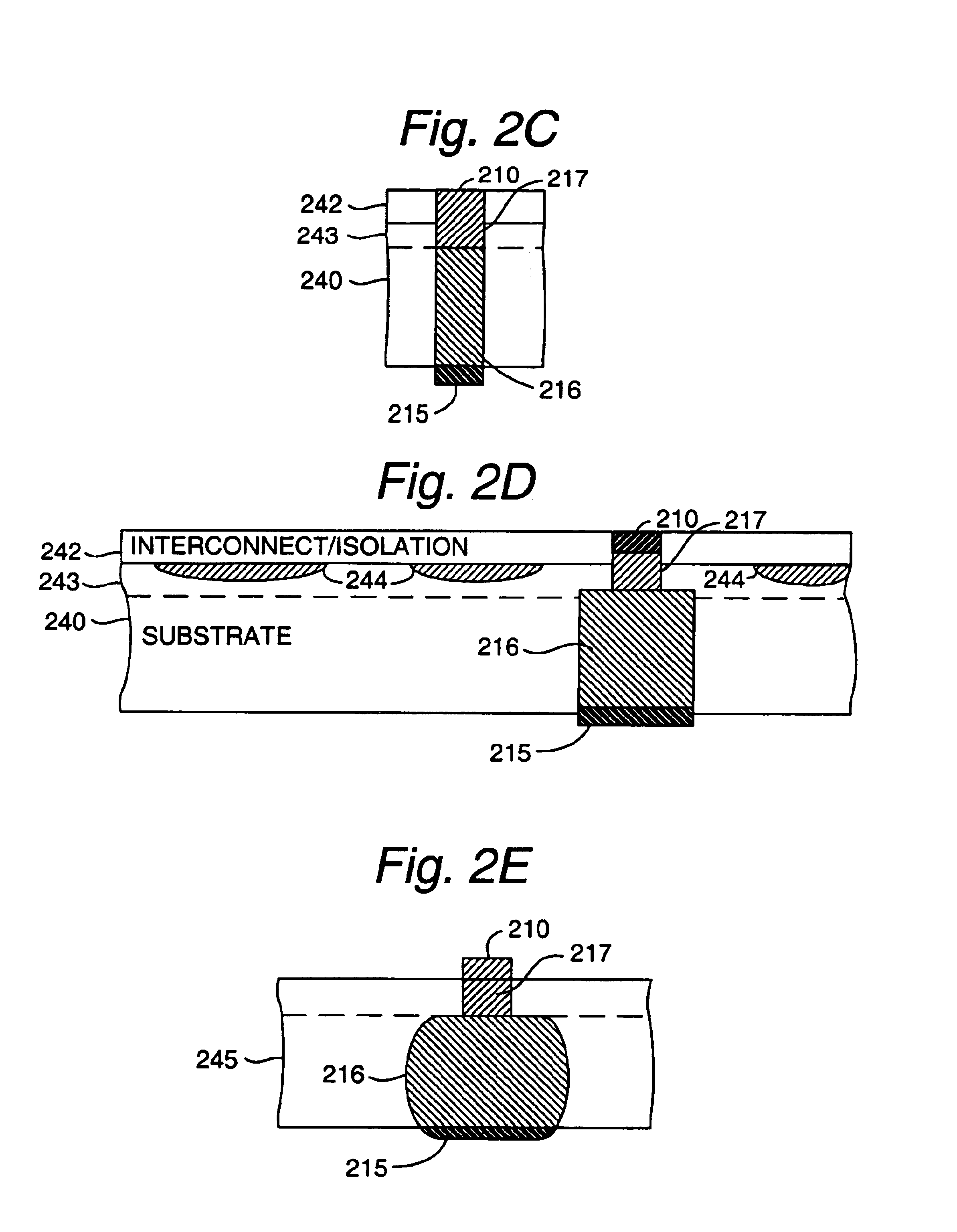
A cross-sectional view of die 230 is illustrated in FIG. 2D. For ease of reference, like numerals refer to like structures from FIG. 2C above. The major difference in this case is of course the shape of via 205, which, in this case, is appropriately shaped to include differently sized top and bottom portions.

first embodiment

A third embodiment of an IC of the present invention is illustrated in FIG. 2E. The primary difference to the first embodiment is the fact that the bottom portion of via 205 is formed to be conical or hemispherically shaped. This structure has operational benefits and processing simplicities that may make it attractive for certain applications.

Other variations of shapes for via 205 will become apparent to those skilled in the art from the present disclosure, and the present invention is by no means limited to any particular implementation.

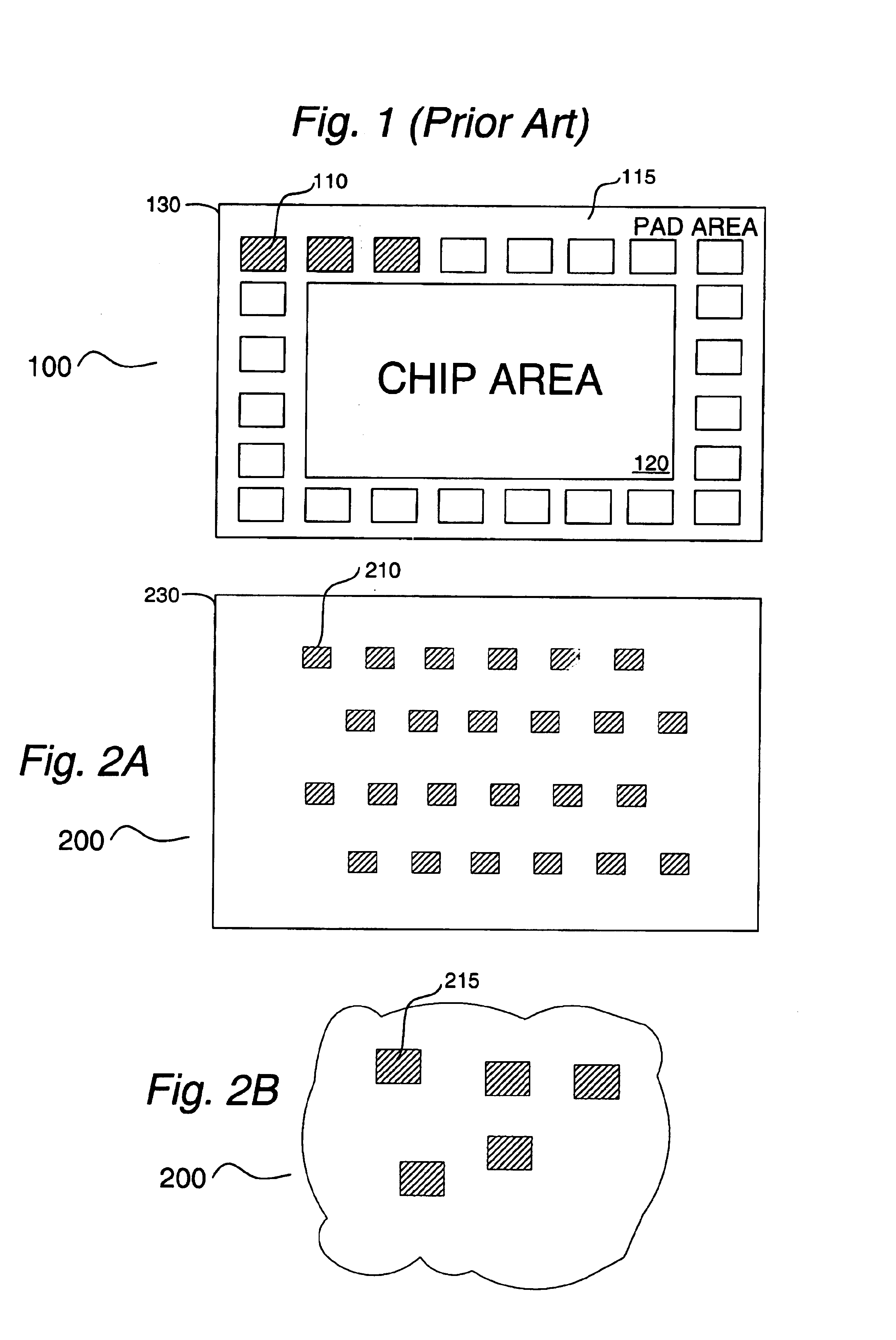
Examples of highly integrated electronic circuits formed in accordance with the present invention is illustrated in FIGS. 3A to 3D. In FIG. 3A, an embodiment of an IC in which both top side interconnects 310 and bottom side interconnects 350 is depicted. As mentioned earlier, such interconnects can include traditional bonding pads, bumps, tape automated bonding, and other conventional structures. A further embodiment shown in FIG. 3B includes bumps...


PUM


Abstract

A semiconductor die and an associated low resistance interconnect located primarily on the bottom surface of such die is disclosed. This arrangement provides a flexible packaging structure permitting easy interconnected with other integrated circuits; in this manner, a number of such circuits can be stacked to create high circuit density multi-chip modules. A process for making the device is further disclosed. To preserve structural integrity of a wafer containing such die during manufacturing, a through-hole via formed as part of the interconnect is filled with an inert material during operations associated with subsequent active device formation on such die.

Description

FIELD OF THE INVENTIONThe invention relates generally to the area of semiconductor device interconnects and packaging techniques. More particularly, the invention discloses an integrated circuit die that is formed with controllable sized and spaced through-holes extending through a substrate of such die, so that such die can be easily and optimally interconnected and packaged.BACKGROUND OF THE INVENTIONContemporary integrated circuits (ICs) include collections of interconnected electronic circuits embodied in semiconductor structures formed during processing of a silicon substrate wafer. The formation of a particular IC can require several hundred discrete complex processing steps within a fab, and is carefully controlled and monitored to ensure a high yield of good die for any particular wafer being processed. With all other things being equal, from a device performance perspective, interconnections between distinct logical circuit areas should be as short as possible. In this way,...

Claims


Application Information

Patent Timeline
Patent Type & Authority Patents(United States)
IPC IPC(8): H01L23/48H01L25/065
CPCH01L23/481H01L2224/16H01L25/0657H01L2224/05001H01L2224/05009H01L2224/05568H01L2224/0557H01L2224/05573H01L2224/0615H01L2224/13025H01L2924/00014H01L2224/05644H01L2224/05647H01L2224/05099
Inventor HSUAN, MIN-CHIH JOHN
Owner UNITED MICROELECTRONICS CORP
Why Eureka
Try Eureka