Superjunction semiconductor device

Active Publication Date: 2005-06-02
SEMICON COMPONENTS IND LLC
View PDF99 Cites 68 Cited by
  • Summary
  • Abstract
  • Description
  • Claims
  • Application Information

AI Technical Summary

Benefits of technology

[0008] In accordance with an aspect of the present invention, a superjunction semiconductor device has a terminati

Problems solved by technology

However, the high resistivity and the relatively large thickness of the drift layer increase the on-resistance of the device.
A higher on-resistance adversely affects the performance of the device by increasing the conduction loss and lowering the switching speed.
Despite the above advantages, the superjunction semiconductor device has a drawback in that it is difficult to stably implement a termination region surrounding the act

Method used


Image

  • Superjunction semiconductor device
  • Superjunction semiconductor device
  • Superjunction semiconductor device

Examples


Embodiment Construction

[0017] This invention may, however, be embodied in many different forms and should not be construed as being limited to the embodiments set forth herein.

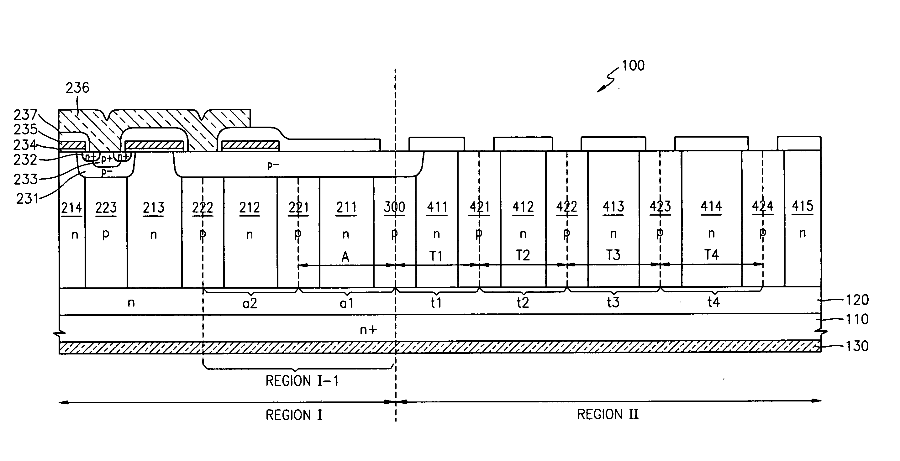
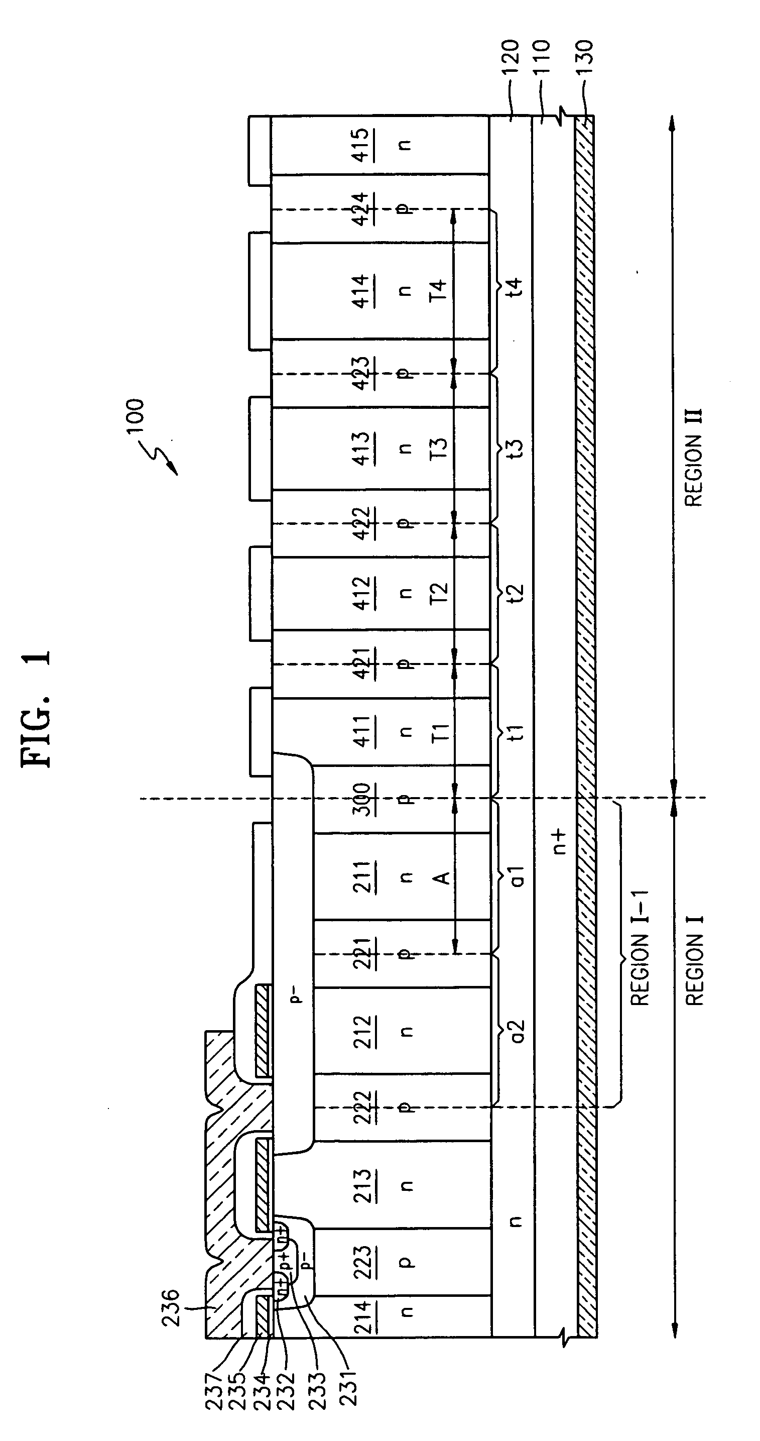
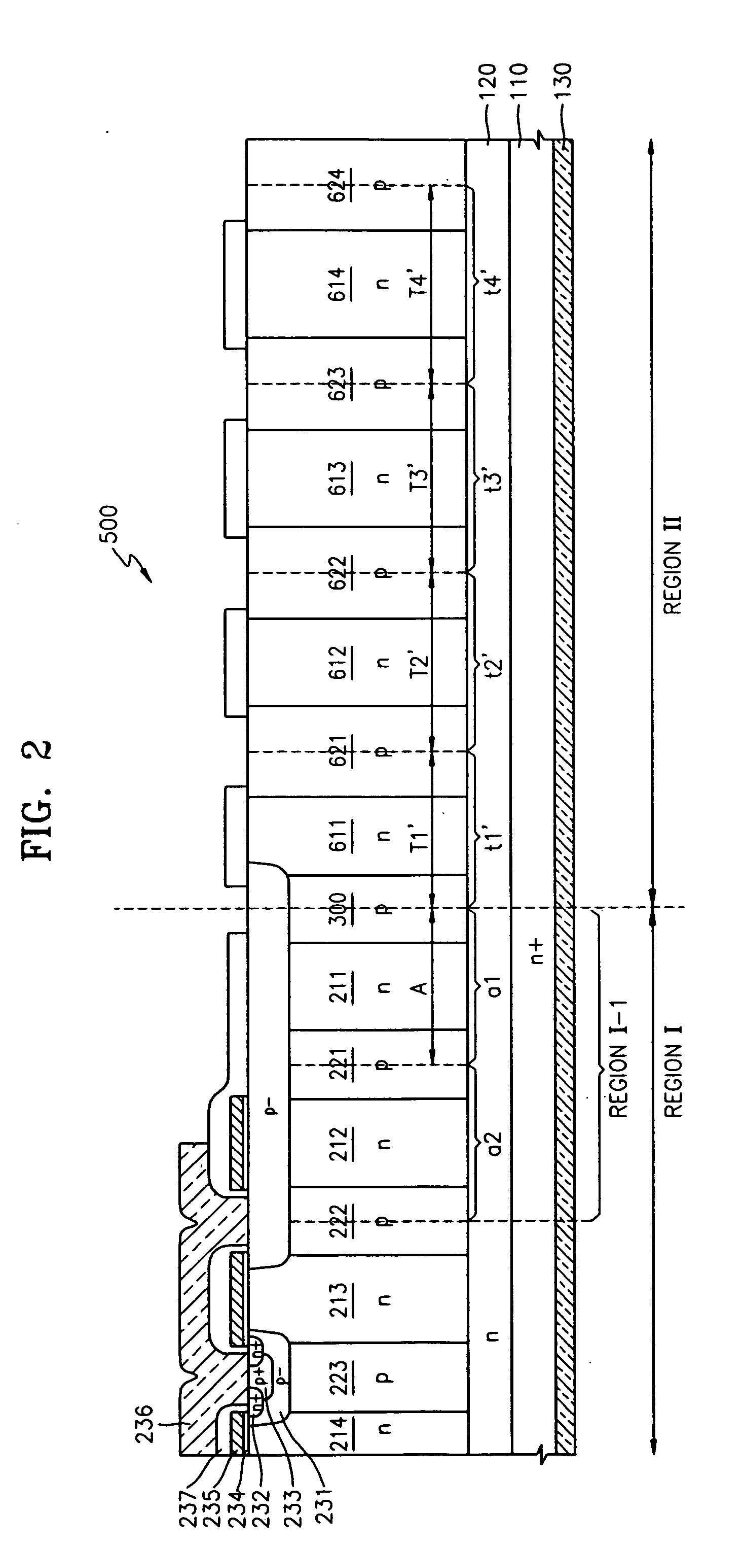
[0018] Referring to FIG. 1, a superjunction semiconductor device 100 according to an embodiment of this invention includes an active region I and a termination region II. Although it is not shown in FIG. 1, termination region II surrounds an edge region I-1. In general, edge region I-1 indicates the outermost region of active region I. In active region I and termination region II, an n-type region 120 is formed on an n-type semiconductor substrate 110 serving as the drain region. A drain electrode 130 is formed on the rear surface of drain region 110.

[0019] Columns of n-type and p-type material are alternately arranged in the lateral direction on n-type region 120 in both active region I and termination region II. Boundary column 300 of p-type material forms the transition region between active region I and termination region II. ...


PUM


Abstract

In accordance with an embodiment of the invention, a superjunction semiconductor device includes an active region and a termination region surrounding the active region. A central vertical axis of a boundary column of a second conductivity type material defines the boundary between the active region and the termination region. The active and termination regions include columns of first and second conductivity type material alternately arranged along a horizontal direction in a semiconductor region having top and bottom surfaces. At least one of the columns of the first conductivity type material in the termination region has a different width than a width of the columns of the first conductivity type material in the active region.

Description

CROSS-REFERENCES TO RELATED APPLICATIONS [0001] This application claims priority from Korean Patent Application No. 2003-85765, filed Nov. 28, 2003, the disclosure of which is incorporated herein by reference in its entirety. BACKGROUND OF THE INVENTION [0002] The present invention relates to a semiconductor device, and more particularly to a superjunction semiconductor device having alternating columns of p-type and n-type conductivity type material in the active and termination regions. [0003] Typically, in vertically conducting semiconductor devices the electrodes are disposed on two opposing planes. When the vertical semiconductor device is turned on, drift current flows along the thickness (i.e., vertical direction) of the semiconductor device. When the device is turned off, depletion regions extend vertically. To realize high breakdown voltage for a vertical semiconductor device, a drift layer between the electrodes must be made from a high resistivity material and have a rela...

Claims


Application Information

Patent Timeline
IPC IPC(8): H01L29/00H01L29/06H01L29/78
CPCH01L29/7802H01L29/0634H01L29/7811H01L29/78
Inventor LEE, JAE-GILJUNG, JIN-YOUNGJANG, HO-CHEOL
Owner SEMICON COMPONENTS IND LLC
Why Eureka
Try Eureka