FinFET SRAM cell using low mobility plane for cell stability and method for forming

a technology of cell stability and sram cell, applied in the field of forming methods of fin field effect transistors, can solve the problems of affecting the performance and/or reliability of the device, unable to achieve the effect of achieving the effect of high gain, low gain, and high gain

Inactive Publication Date: 2005-06-09
GLOBALFOUNDRIES INC
View PDF13 Cites 215 Cited by
  • Summary
  • Abstract
  • Description
  • Claims
  • Application Information

AI Technical Summary

Benefits of technology

[0010] Accordingly, the present invention provides a device design and method for forming the same that results in Fin Field Effect Transistors having different gains without negatively impacting device density. The present invention forms relatively low gain F...

Problems solved by technology

FETs are used in almost all types of integrated circuit design (i.e., microprocessors, memory, etc.) Unfortunately, increased device density in CMOS FET often results in degradation of performance and/or reliability.
Unfortunately, several difficulties arise in the design and fabrication of FinFET transistors.
For example, there has been no efficient method for creating FinFETs having different gains on the same d...

Method used


Image

  • FinFET SRAM cell using low mobility plane for cell stability and method for forming
  • FinFET SRAM cell using low mobility plane for cell stability and method for forming
  • FinFET SRAM cell using low mobility plane for cell stability and method for forming

Examples


Embodiment Construction

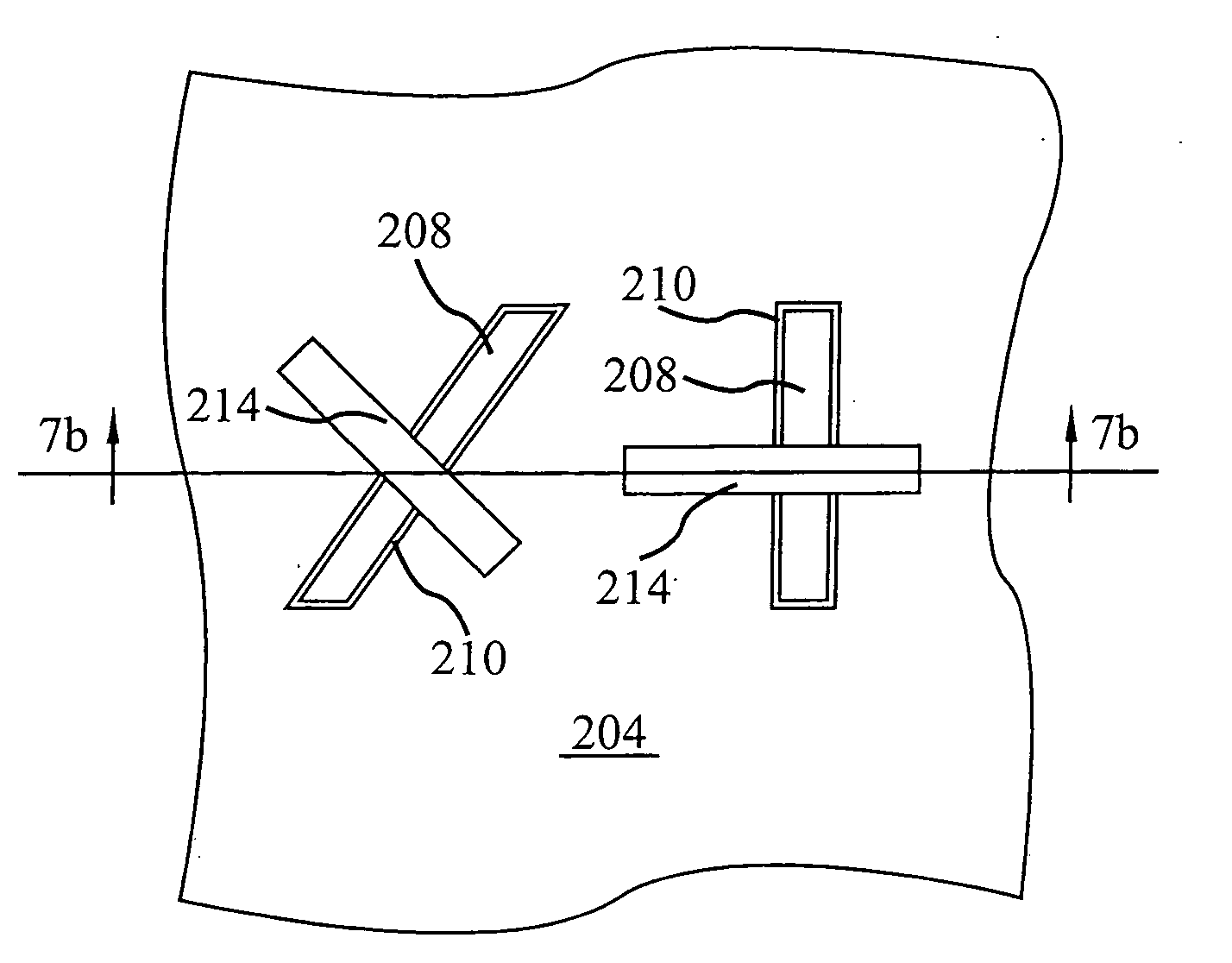
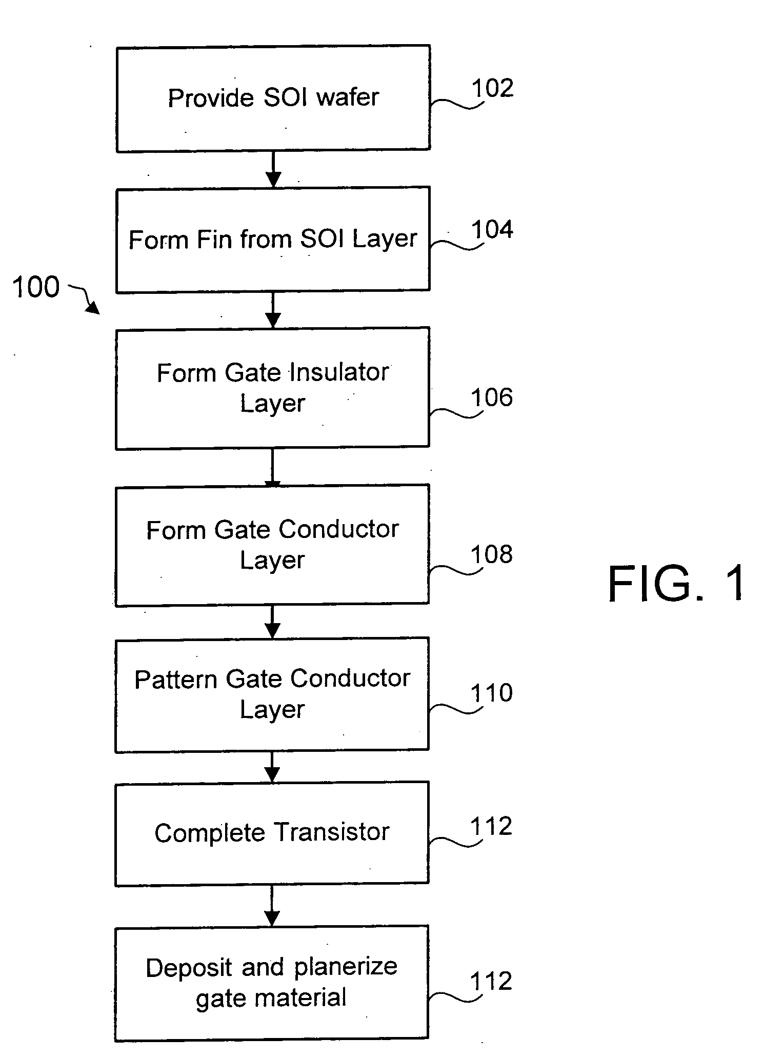
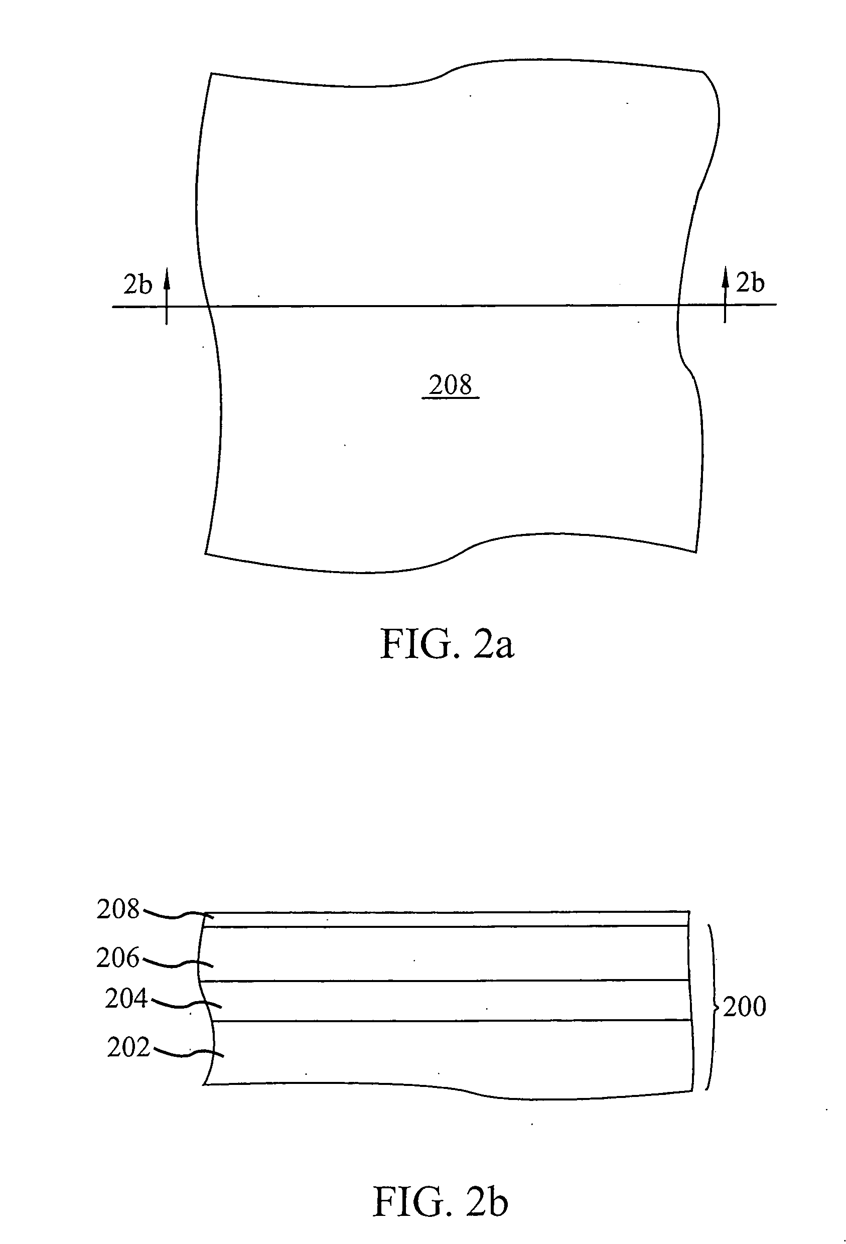
[0020] As discussed above, the present invention exploits semiconductor physics by utilizing different crystal planes for FinFET transistors that results in FinFET having different gains without overly impacting negative device density. The present invention forms relatively low gain FinFET transistors in a low carrier mobility plane and relatively high gain FinFET transistors in a high carrier mobility plane. Thus formed, the FinFETs formed in the high mobility plane have a relatively higher gain than the FinFETs formed in the low mobility plane. Individuals skilled in the art of semiconductor physics may wish to proceed with to the Detailed Description section of this specification. However, those individuals who are new to crystal lattice planes and directions, should read the following Overview section in order to best understand the benefits and advantages of the present invention.

Overview

[0021] In crystalline solids, the atoms which make up the solid are spatially arranged ...


PUM


Abstract

The present invention provides a device design and method for forming the same that results in Fin Field Effect Transistors having different gains without negatively impacting device density. The present invention forms relatively low gain FinFET transistors in a low carrier mobility plane and relatively high gain FinFET transistors in a high carrier mobility plane. Thus formed, the FinFETs formed in the high mobility plane have a relatively higher gain than the FinFETs formed in the low mobility plane. The embodiments are of particular application to the design and fabrication of a Static Random Access Memory (SRAM) cell. In this application, the bodies of the n-type FinFETs used as transfer devices are formed along the {110} plane. The bodies of the n-type FinFETs and p-type FinFETs used as the storage latch are formed along the {100}. Thus formed, the transfer devices will have a gain approximately half that of the n-type storage latch devices, facilitating proper SRAM operation

Description

BACKGROUND OF THE INVENTION [0001] 1. Technical Field [0002] The present invention relates generally to the field of semiconductor manufacturing and, more specifically, to a method for Fin field effect transistors having different gains. [0003] 2. Background Art [0004] The need to remain cost and performance competitive in the production of semiconductor devices has caused continually increasing device density in integrated circuits. To facilitate the increase in device density, new technologies are constantly needed to allow the feature size of these semiconductor devices to be reduced. [0005] The push for ever increasing device densities is particularly strong in CMOS technologies, such as the in the design and fabrication of field effect transistors (FETs). FETs are used in almost all types of integrated circuit design (i.e., microprocessors, memory, etc.) Unfortunately, increased device density in CMOS FET often results in degradation of performance and / or reliability. [0006] On...

Claims


Application Information

Patent Timeline
IPC IPC(8): H01L21/8244H01L21/84H01L27/12
CPCH01L21/84H01L27/11Y10S257/903H01L29/785H01L27/1203H10B10/00
Inventor FRIED, DAVID M.MANN, RANDY W.MULLER, K. PAULNOWAK, EDWARD J.
Owner GLOBALFOUNDRIES INC
Why Eureka
Try Eureka