Method of forming a semiconductor device with a high dielectric constant material and an offset spacer

a technology of dielectric constant material and offset spacer, which is applied in the direction of semiconductor devices, electrical appliances, transistors, etc., can solve the problems of high unwanted leakage current, needing an additional and costly process step, etc., and achieve the effect of reducing the number of fabrication steps

Inactive Publication Date: 2005-06-09
TAIWAN SEMICON MFG CO LTD
View PDF7 Cites 22 Cited by
  • Summary
  • Abstract
  • Description
  • Claims
  • Application Information

AI Technical Summary

Benefits of technology

[0007] It is another object of this invention to minimize fabrication steps by integrating the removal of

Problems solved by technology

The reduction in thickness for gate insulator layers such as silicon dioxide, can however result in higher unwanted leakage currents when compared to thicker gate insulator counterparts.
If the high k layer is used as a gate insulator layer

Method used


Image

  • Method of forming a semiconductor device with a high dielectric constant material and an offset spacer
  • Method of forming a semiconductor device with a high dielectric constant material and an offset spacer
  • Method of forming a semiconductor device with a high dielectric constant material and an offset spacer

Examples


Embodiment Construction

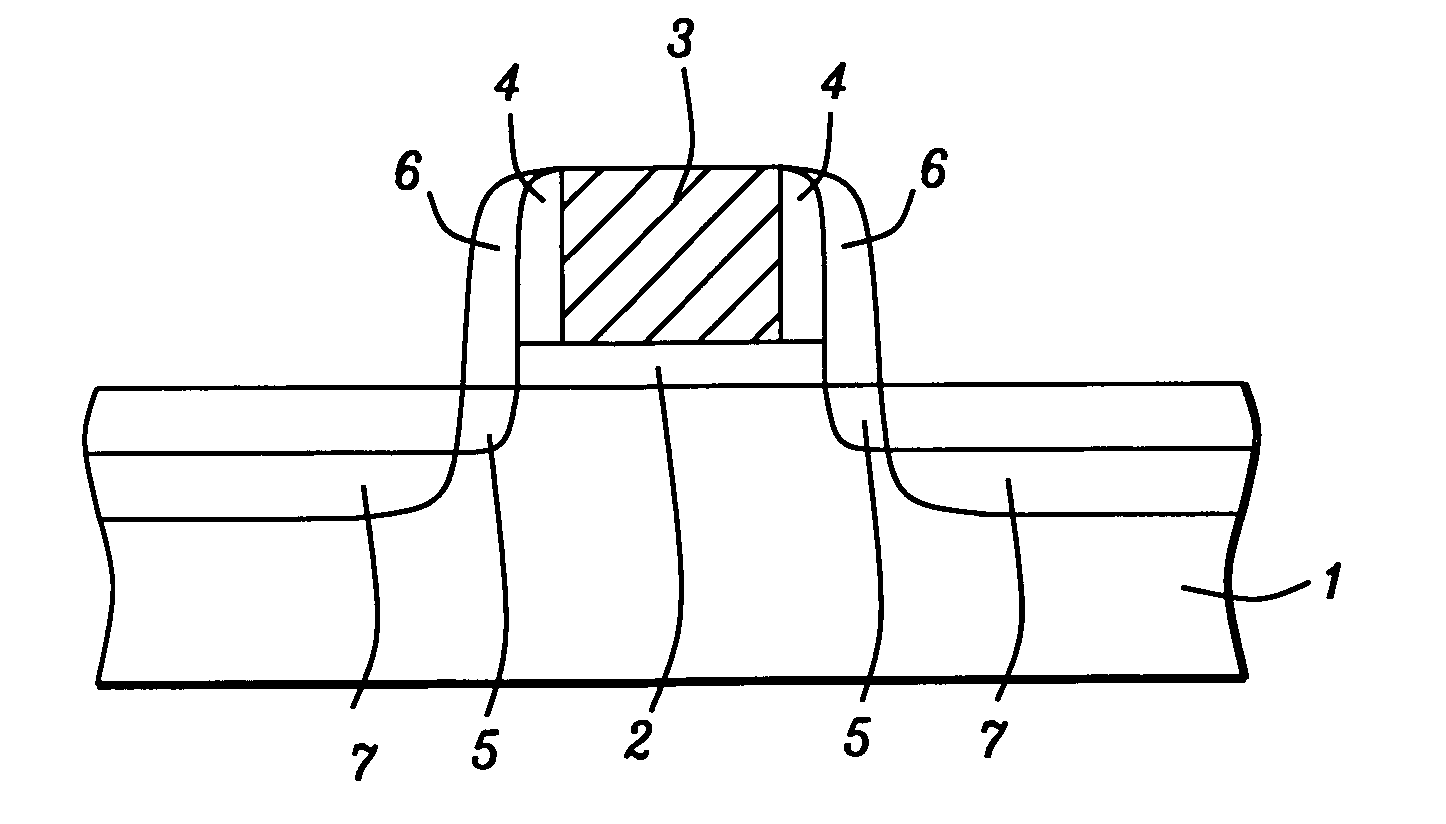
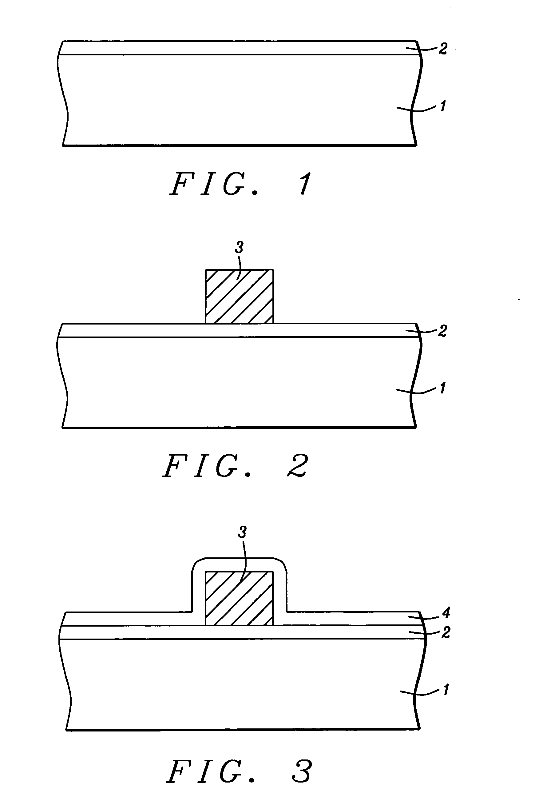
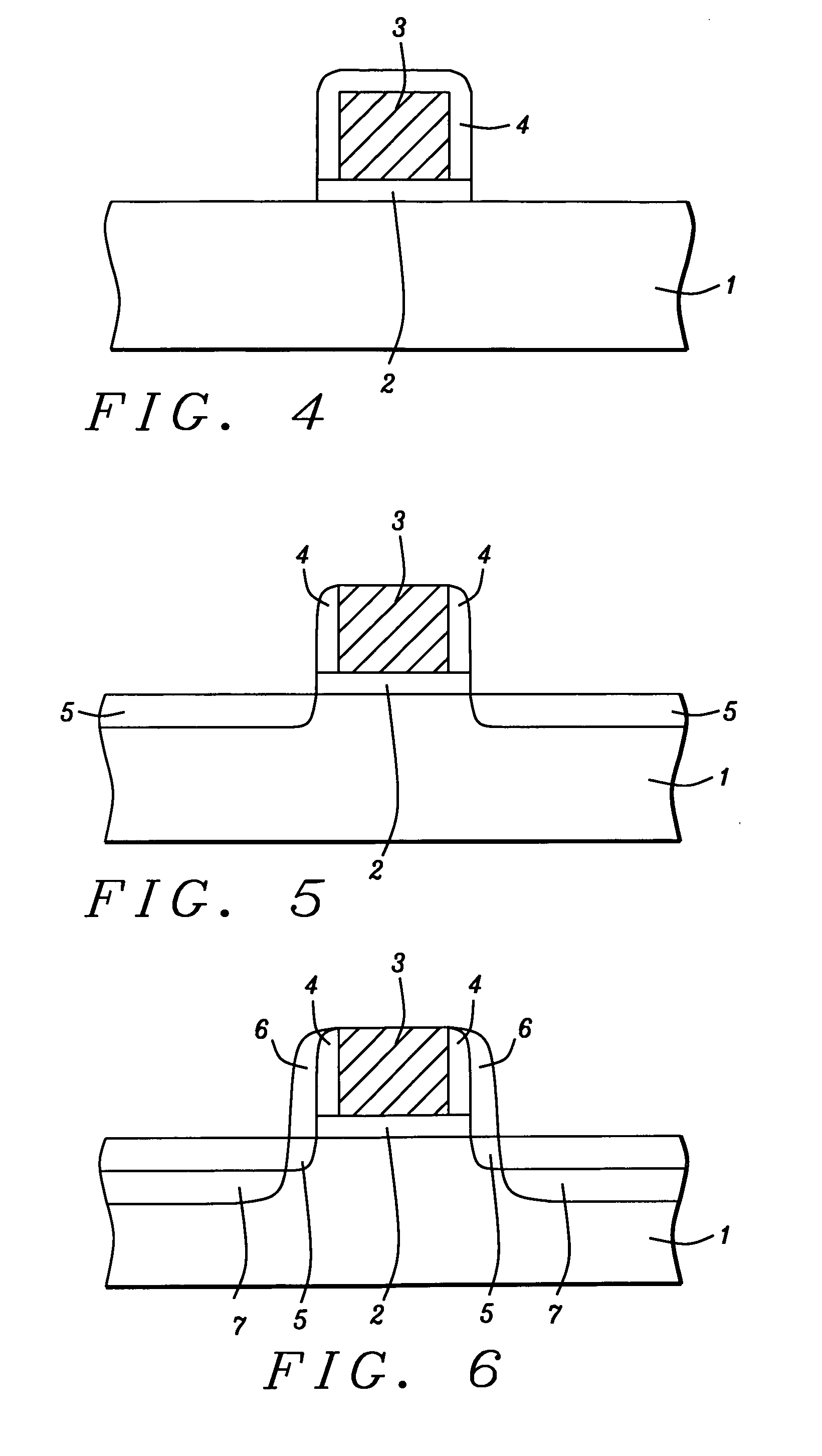
[0012] The method of fabricating a MOSFET device wherein the definition of an insulator offset spacer located on the sides of a conductive gate structure, and the removal of unwanted portions of a high k gate insulator layer, both accomplished via a single dry etch procedure, will now be described in detail. Semiconductor substrate 1, comprised of P type single crystalline silicon featuring a crystallographic orientation, is used and schematically shown in FIG. 1. Isolation regions, not shown in the drawings, are formed in top portions of non-device regions of semiconductor substrate 1. Isolation regions can be either thermally oxidized field oxide (FOX) regions, or insulator filled shallow trench isolation (STI) regions. Attempts to maximize device performance can be directed to numerous components of a device. For example MOSFET device performance can be increased with decreasing gate insulator thickness. However gate insulator layers comprised of silicon dioxide with a dielectri...


PUM


Abstract

A process sequence for forming a MOSFET device featuring a high k gate insulator layer, wherein the use of the high k gate insulator layer requires no additional photolithographic procedures, has been developed. After deposition of a high k gate insulator layer followed by the definition of an overlying conductive gate structure, an insulator layer is deposited. An anisotropic dry etch procedure is then employed to first define offset insulator spacers on the sides of the conductive gate structure, then to selectively remove the unwanted portions of the high k gate insulator layer. The use of the high k gate insulator layer provides a thin gate insulator layer with less risk of leakage when compared to counterpart gate insulator layers such as silicon dioxide, while the integration of the definition of the offset insulator spacer step and of the high k gate layer removal procedure, results in fabrication cost savings.

Description

BACKGROUND OF THE INVENTION [0001] (1) Field of the Invention [0002] The present invention relates to methods used to fabricate semiconductor devices, and more specifically to a method of forming a semiconductor device featuring a high dielectric constant (high k) gate insulator layer and an offset sidewall spacer. [0003] (2) Description of Prior Art [0004] The quest to continually improve semiconductor device performance has emphasized the use of sub-0.25 um features for metal oxide semiconductor field effect transistor (MOSFET) devices. In addition to further improve MOSFET performance and to reduce operating voltage, the thickness of the MOSFET gate insulator layer has continually been reduced. The reduction in thickness for gate insulator layers such as silicon dioxide, can however result in higher unwanted leakage currents when compared to thicker gate insulator counterparts. Therefore to maintain a thin gate insulator layer with reduced risk of leakage high k layers can be use...

Claims


Application Information

Patent Timeline
IPC IPC(8): H01L21/336H01L29/78H01L29/94H01L31/062
CPCH01L29/6656H01L29/7833H01L29/6659
Inventor CHEN, FANG-CHENGTSAI, MING-HUNGLIN, HUN-JERCHIU, YUNG-HUNG
Owner TAIWAN SEMICON MFG CO LTD
Why Eureka
Try Eureka