Semiconductor device and testing method thereof

a technology of semiconductor devices and testing methods, applied in static indicating devices, solid-state devices, instruments, etc., to achieve the effect of reducing the testing/manufacturing cost of semiconductor devices and reducing the time required

Inactive Publication Date: 2005-06-09
RENESAS ELECTRONICS CORP
View PDF5 Cites 33 Cited by
  • Summary
  • Abstract
  • Description
  • Claims
  • Application Information

AI Technical Summary

Benefits of technology

[0010] (1) Since output voltage measurement (analog voltage measurement) is performed by the ATE (tester), it takes long until the output voltage is stabilized, and therefore, the testing time is increased.
[0013] An object of the present invention is to provide the technique capable of solving the problems mentioned above and reducing the time required for the gray-scale voltage test of a semiconductor device provided with a driver circuit of a liquid crystal display. Also, another object thereof is to provide the technique that can reduce the cost of testing / manufacturing a semiconductor device provided with a driver circuit of a liquid crystal display.
[0022] According to the present invention, it is possible to reduce the time required for the gray-scale voltage test of the semiconductor device provided with a driver circuit of a liquid crystal display (liquid crystal driver circuit).
[0023] In addition, it is also possible to reduce the testing / manufacturing cost of the semiconductor device provided with a driver circuit of a liquid crystal display.

Problems solved by technology

However, the technique described in Japanese Patent Application Laid-Open No. 2002-156412 has the following problems:

Method used


Image

  • Semiconductor device and testing method thereof
  • Semiconductor device and testing method thereof
  • Semiconductor device and testing method thereof

Examples


first embodiment

(FIRST EMBODIMENT)

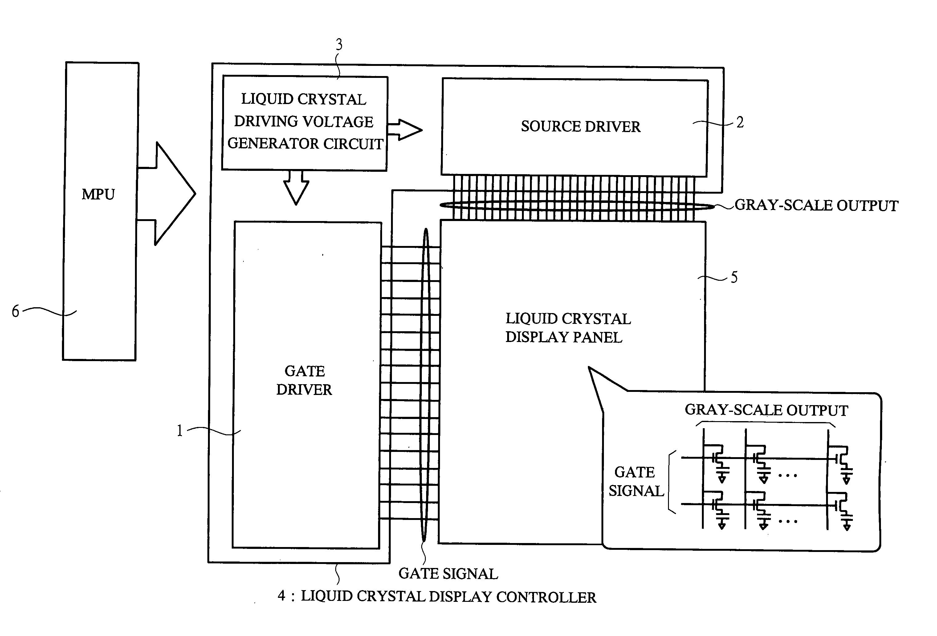
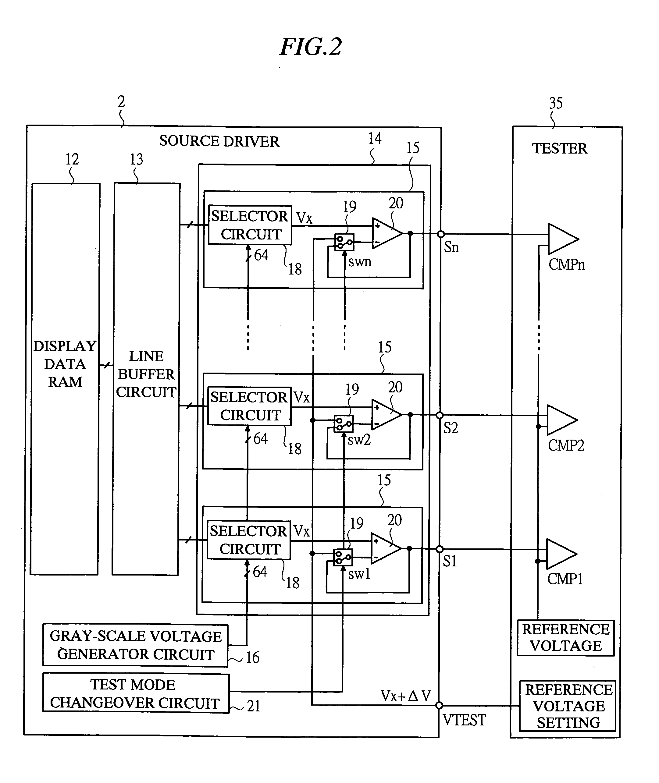
[0039]FIG. 2 shows configuration of the semiconductor device having a liquid crystal driver circuit in the first embodiment of the present invention. As the first embodiment of the present invention, FIG. 2 shows the case where the semiconductor device having a liquid crystal driver circuit is composed of the source driver (which corresponds to the configuration of (1) described above). More specifically, the liquid crystal driver circuit in the semiconductor device of the first embodiment is the source driver 2 shown in FIG. 1.

[0040] In FIG. 2, the source driver 2 is composed of a display data RAM 12 that stores data to be written or read via an external interface, a line buffer circuit 13 that retains data written in the display data RAM 12, a gray-scale voltage generator circuit 16 that generates gray-scale voltage at a predetermined level, a gray-scale voltage selector circuit 14 that outputs gray-scale voltage in accordance with gray-scale setting data retain...

second embodiment

(SECOND EMBODIMENT)

[0065] Subsequently, as a semiconductor device having a liquid crystal driver circuit in the second embodiment of the present invention, configuration and one example of the operation in the case where a reference voltage generator circuit is arranged within a display controller will be described. FIG. 5 shows configuration of a semiconductor device having the reference voltage generator circuit (the reference voltage generator circuit 22 in the figure) arranged within the source driver.

[0066] The liquid crystal driver circuit in the semiconductor device of the second embodiment is applied to, for example, the source driver 2 shown in FIG. 1.

[0067] The liquid crystal display controller 4 including this source driver 2 is composed of a display data RAM 12 that stores data written or read through an external interface, a line buffer circuit 13 that retains data written to the display data RAM 12, a gray-scale voltage generator circuit 16 that generates gray-scale ...


PUM

PropertyMeasurementUnit
voltageaaaaaaaaaa
gray-scale voltageaaaaaaaaaa
reference voltageaaaaaaaaaa

Abstract

A semiconductor device according to the present invention has a liquid crystal driver circuit, and when gray-scale voltage thereof is tested, the gray-scale voltage (Vx) generated in a gray-scale voltage generator circuit provided therein is compared with reference voltage (e.g., Vx+ΔV) generated for testing the gray-scale voltage and the test result is output as binarized voltage from external terminals of the semiconductor device. This can speed up the gray-scale voltage test even in the case of higher gray scale in the liquid crystal driver circuit or increased number of output terminals of the semiconductor device. Therefore, it becomes possible to reduce the time and cost required for the test.

Description

[0001] The present application claims priority from Japanese application JP 2003-378595 filed on Nov. 07, 2003 and Japanese application JP 2004-310341 filed on Oct. 26, 2004 the contents of which are hereby incorporated by reference into this application. BACKGROUND OF THE INVENTION [0002] 1. Field of the Invention [0003] The present invention relates to a semiconductor device and a testing method thereof, and more particularly, it relates to a semiconductor device having a number of external terminals (output terminals) and a testing method for testing output voltage thereof. [0004] 2. Description of the Related Art [0005] A semiconductor device provided with a driver circuit of a liquid crystal display (also referred to as a liquid crystal driver circuit, or LCD driver) drives the liquid crystal display (liquid crystal panel) by outputting multi-stage (multiple gray-scale) voltage from a number of external terminals (output pins). [0006] Conventionally, a gray-scale voltage test o...

Claims


Application Information

Patent Timeline
Patent Type & Authority Applications(United States)
IPC IPC(8): G01R31/28G01R31/316G02F1/133G09G3/00G09G3/20G09G3/36H01L21/822H01L27/04
CPCG09G3/3688G09G3/006
Inventor MAKUUCHI, MASAMICHUJO, NORIOIMAGAWA, KENGOORIHASHI, RITSUROARAI, YOSHITOMO
Owner RENESAS ELECTRONICS CORP
Why Eureka
Try Eureka