Mask and method for manufacturing the same, method for manufacturing display, method for manufacturing organic electroluminescent display, organic electroluminescent device, and electronic device

a technology of mask and glass, which is applied in the direction of photomechanical equipment, instruments, and semiconductor/solid-state device details, etc., can solve the problems of glass substrate not being able the silicon mask and the glass substrate may not be able to meet the needs of evaporation objects, and the glass substrate cannot be made to come in close contact with the silicon mask without a permanent magnet, etc., to achieve excellent display performance

Inactive Publication Date: 2005-06-09
SEIKO EPSON CORP
View PDF11 Cites 23 Cited by
  • Summary
  • Abstract
  • Description
  • Claims
  • Application Information

AI Technical Summary

Benefits of technology

[0032] According to the present invention, a high-quality display, an organic electroluminescent display, and an electronic device which include a precisely pa

Problems solved by technology

As a result, misalignment between through-holes (openings) provided in the metal mask and the evaporation object may occur, especially at the edges of the glass substrate.
However, the glass substrate cannot be made to come in a close contact with the silicon mask without a permanent magnet.
Furthermore, as the sizes of the silicon mask and the glass substrate increase, the bending deformations (distortion deformation

Method used


Image

  • Mask and method for manufacturing the same, method for manufacturing display, method for manufacturing organic electroluminescent display, organic electroluminescent device, and electronic device
  • Mask and method for manufacturing the same, method for manufacturing display, method for manufacturing organic electroluminescent display, organic electroluminescent device, and electronic device
  • Mask and method for manufacturing the same, method for manufacturing display, method for manufacturing organic electroluminescent display, organic electroluminescent device, and electronic device

Examples


Embodiment Construction

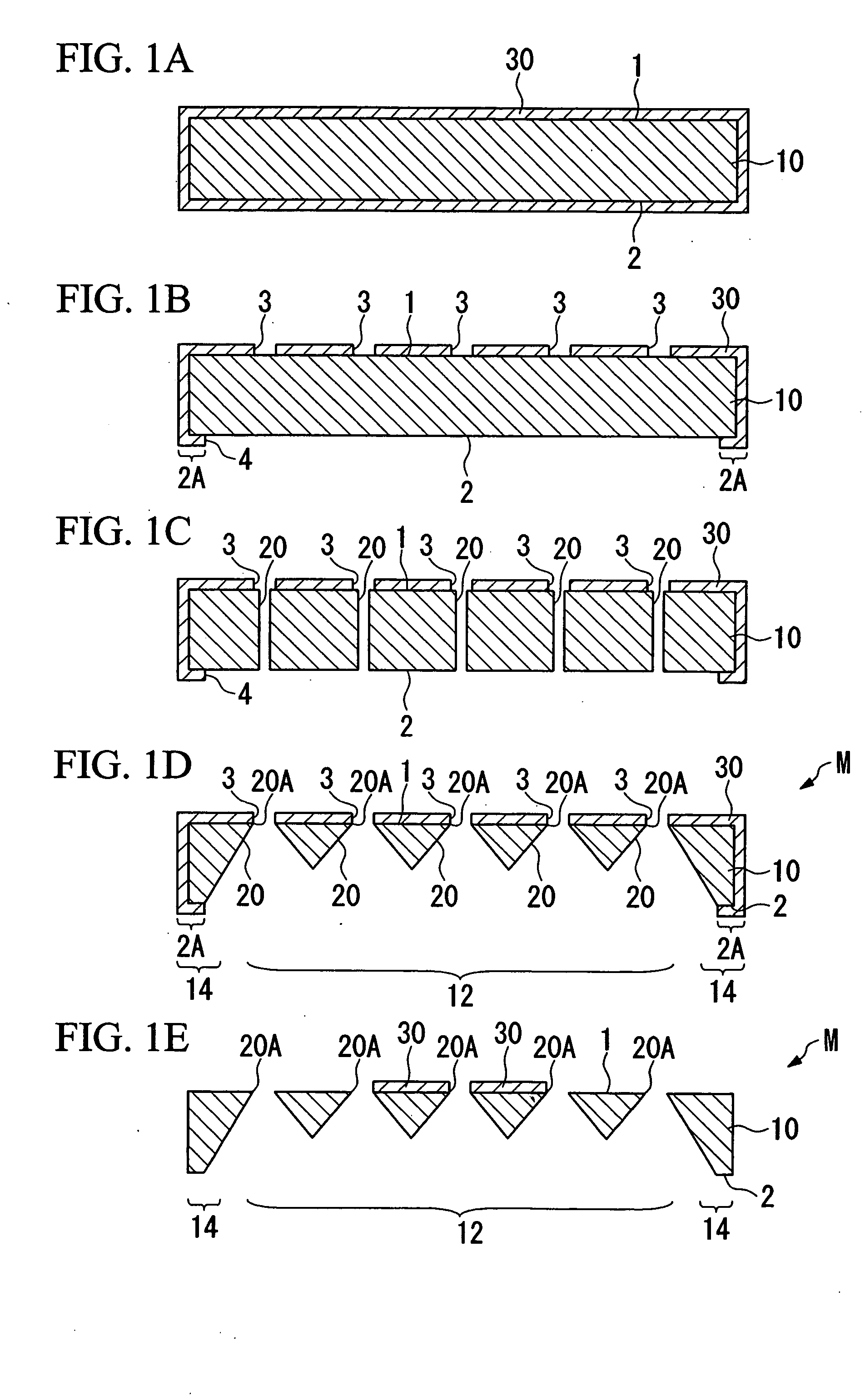
[0043] Hereinafter, one embodiment of a method for manufacturing a mask according to the present invention will be explained with reference to FIG. 1.

[0044]FIGS. 1A to 1E schematically illustrate a process for manufacturing the mask according to the present invention.

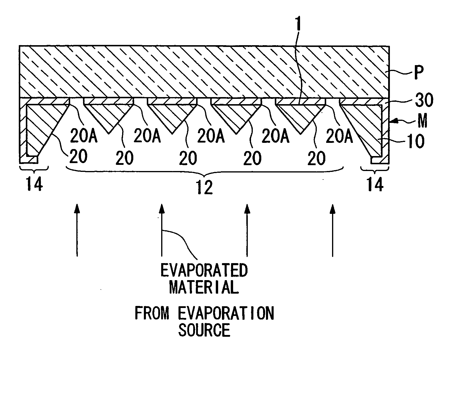
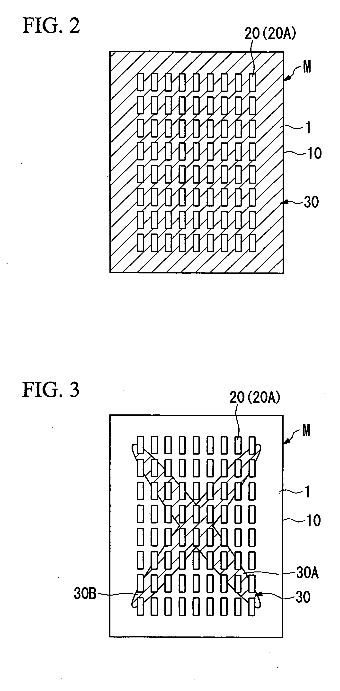
[0045] First, a substrate 10 which is a base material of a mask M is provided as shown in FIG. 1A. The substrate 10 is made of silicon (Si), and more specifically is made of single crystal silicon (single crystal Si). In this embodiment, a first side (i.e., front side) 1 and a second side (i.e., back side) 2 of the silicon substrate 10 are surfaces having a Miller index of (100).

[0046] In the first step, an anti-etching film 30 is provided on the silicon substrate 10.

[0047] The anti-etching film 30 is provided on at least the first side 1 of the silicon substrate 10. It should be noted that the anti-etching film 30 may also be provided on the second side 2. In the example shown in FIG. 1A, the anti-etching film 30 i...


PUM

PropertyMeasurementUnit
Thicknessaaaaaaaaaa
Shapeaaaaaaaaaa
Stress optical coefficientaaaaaaaaaa

Abstract

A mask includes a substrate which includes a front side and a back side and is provided with through-holes; and a film which adjusts a shape of the substrate provided above at least one of the front side and the back side of the substrate. A method of manufacturing a mask includes the steps of: providing a substrate having a front side and a back side; forming a film which adjusts a shape of the substrate above at least one of the front side and the back side of the substrate; and drilling through-holes in the substrate.

Description

BACKGROUND OF THE INVENTION [0001] 1. Field of the Invention [0002] The present invention relates to a mask and a method for manufacturing a mask, to a method for manufacturing a display, to a method for manufacturing an organic electroluminescent display, to an organic electroluminescent device, and to an electronic device. [0003] Priority is claimed on Japanese Patent Application No. 2003-386511, filed Nov. 17, 2003, the content of which is incorporated herein by reference. [0004] 2. Description of Related Art [0005] In a manufacturing process of low molecular fill-color organic EL (electroluminescent) displays, for example, masks are used to pattern pixels of the display by evaporating organic materials for forming pixels of various colors. Japanese Unexamined Patent Applications, First Publication Nos. 2001-93667 and 2001-185350 disclose one example of a technology for patterning pixels by evaporating organic materials forming pixels of various colors. [0006] The methodology dis...

Claims


Application Information

Patent Timeline
IPC IPC(8): H05B33/10C23C14/04G03F7/12H01L51/50H01L51/56
CPCG03F7/12C23C14/042H05B33/10
Inventor KUWAHARA, TAKAYUKIYOTSUYA, SHINICHI
Owner SEIKO EPSON CORP
Why Eureka
Try Eureka