

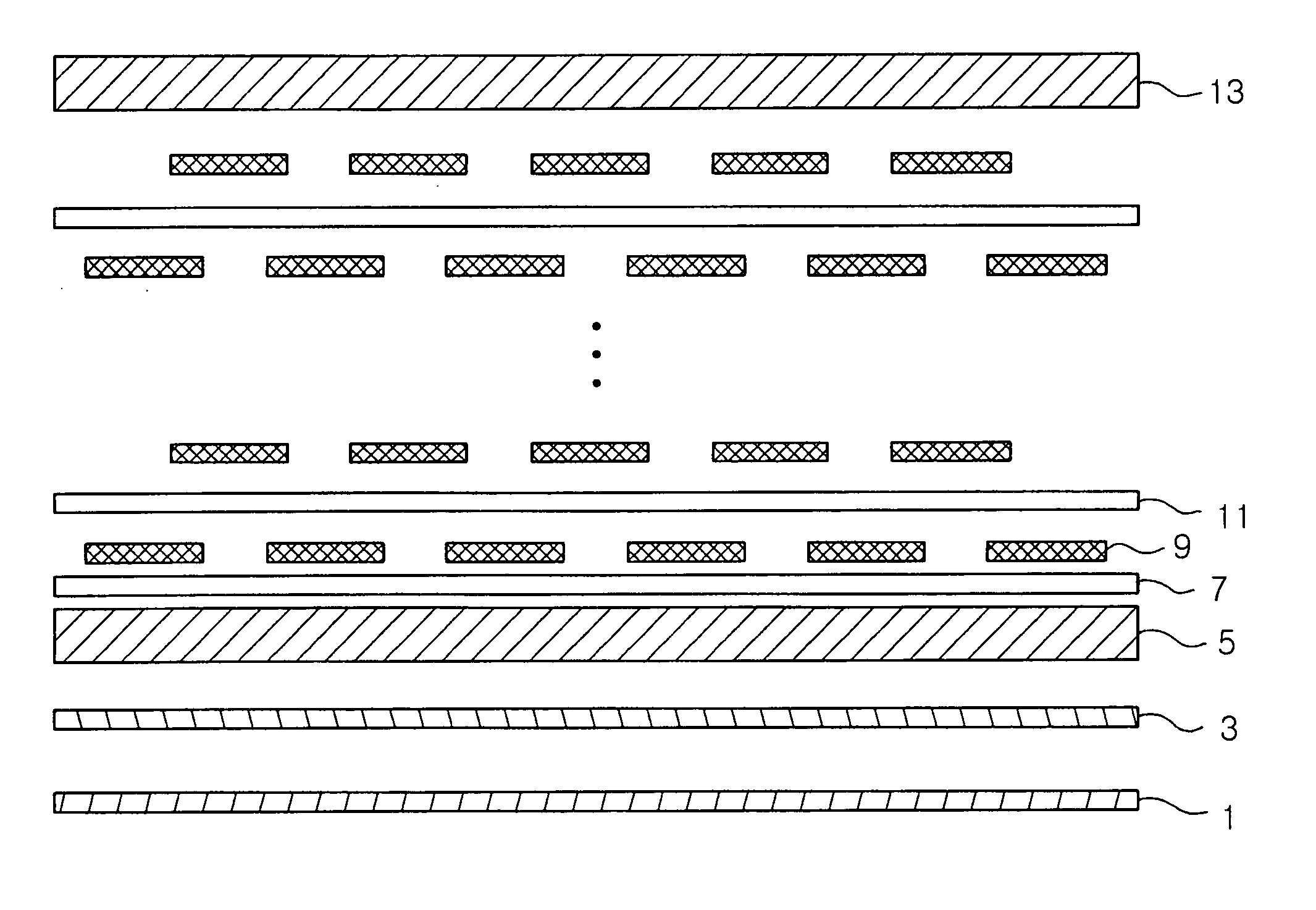
Method of manufacturing multilayered ceramic capacitor by spin coating and multilayered ceramic capacitor
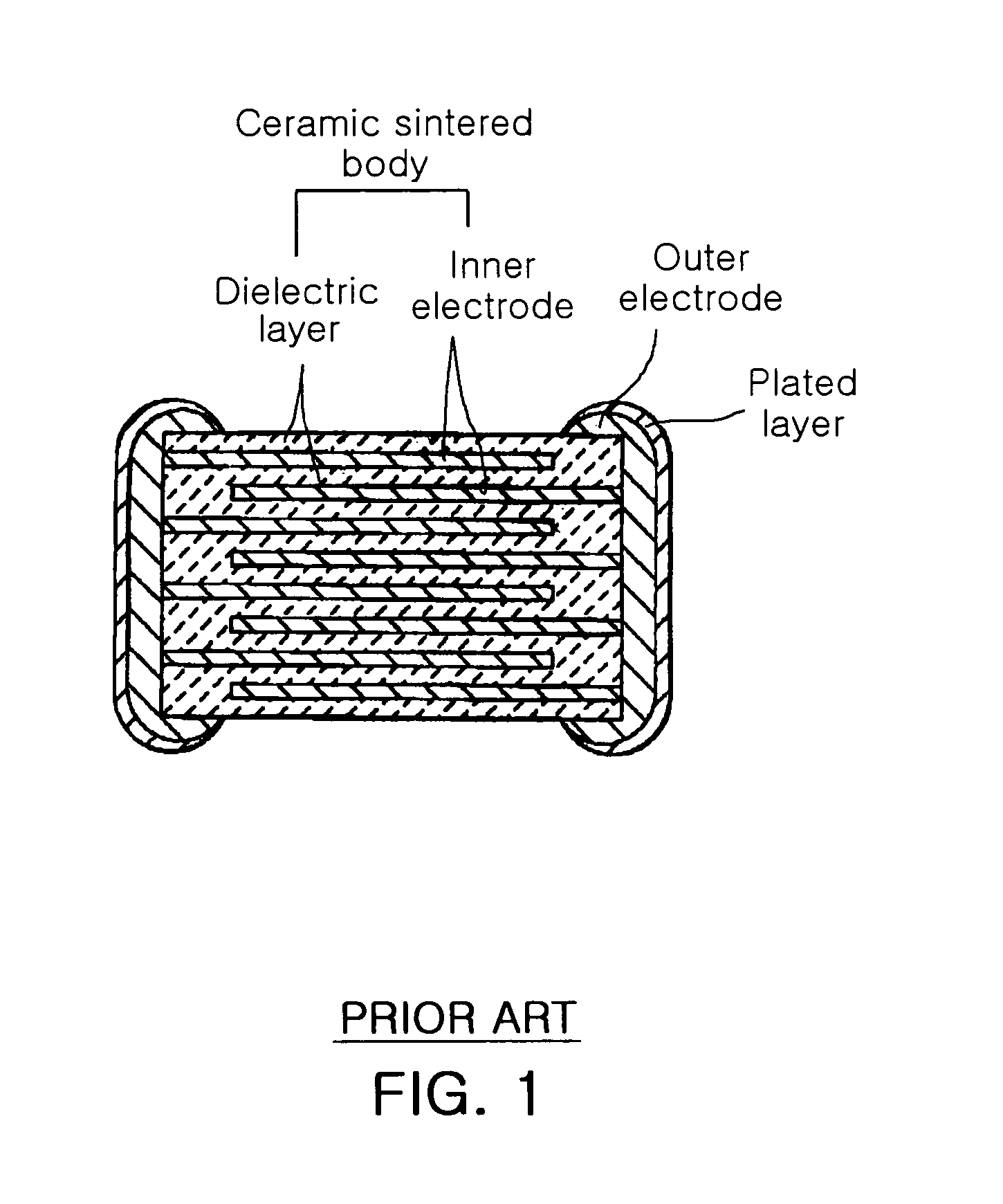
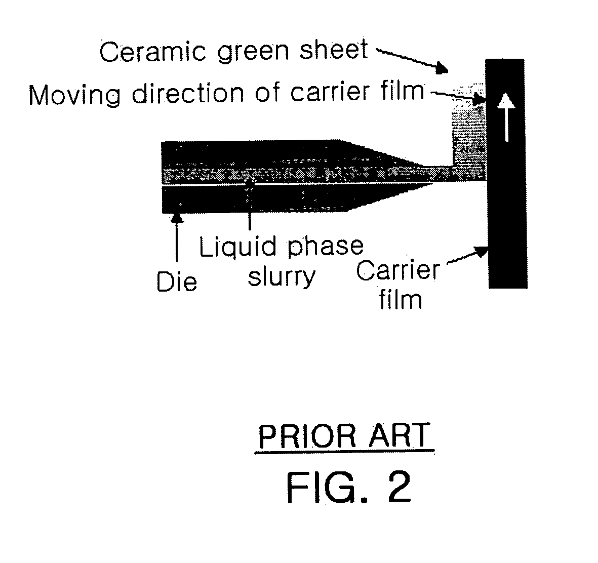
a multi-layer ceramic and capacitor technology, applied in the direction of capacitor manufacturing, fixed capacitor details, fixed capacitors, etc., can solve the problems of difficult to separate the green sheet from the carrier film, the formation of thin dielectric layers is limited by the tape casting process, and the phenomenon of pillowing is difficult to achieve. achieve the effect of preventing the phenomenon of pillowing
- Summary
- Abstract
- Description
- Claims
- Application Information
AI Technical Summary
Benefits of technology
Problems solved by technology
Method used
Image

Examples
example 1
[0068] Preparation of Particulate Sol
[0069] 15-40 wt % BaTiO3 having an average particulate size of 0.05-0.5 μm was admixed with 60-85 wt % 2-methoxy ethanol, to prepare a particulate sol, part of which was subjected to ball milling for 24 hours.
[0070] Preparation of Polymeric Sol
[0071] 5-10 wt % barium acetate was dissolved in 15-30 wt % acetic acid and then stirred, to obtain a barium acetate solution. Separately, 5-10 wt % titanium isoproxide was added to 40-65 wt % 2-methoxy ethanol, to obtain a titanium isoproxide solution. Subsequently, while the barium acetate solution was added one droplet at a time to the titanium isoproxide solution, the two solutions were admixed. At this time, the admixing process was performed to achieve a molar ratio of 1:1. Then, the admixture was further mixed for 1 hour, after which this admixture was added with acetylacetone as a reaction inhibitor to ensure the reaction stability.
[0072] Preparation of Hybrid Sol
[0073] The particulate sol and ...
example 2
[0083] Preparation of Particulate Sol
[0084] 15-40 wt % BaTiO3 powder having an average particulate size of 0.05-0.5 μm was admixed with 60-85 wt % 2-methoxy ethanol (2-MOE), to prepare a particulate sol, part of which was subjected to ball milling for 24 hours.
[0085] Preparation of Polymeric Sol having Polymer
[0086] 5-10 wt % barium acetate was dissolved in 15-30 wt % acetic acid and then stirred, to prepare a barium acetate solution. Separately, 5-10 wt % titanium isoproxide was added to 40-65 wt % 2-methoxy ethanol, to prepare a titanium isoproxide solution.
[0087] Thereafter, while the barium acetate solution was added one droplet at a time to the titanium isoproxide solution, the two solutions were admixed. At this time, the admixing process was carried out to achieve a molar ratio of 1:1. Then, the admixture was additionally mixed for 1 hour, after which the resultant admixture was added with acetylacetone as a reaction inhibitor to ensure the reaction stability. Subsequentl...
PUM
| Property | Measurement | Unit |
|---|---|---|
| thickness | aaaaa | aaaaa |
| thickness | aaaaa | aaaaa |
| thickness | aaaaa | aaaaa |
Abstract
Description
Claims
Application Information